Electrochemical Plating (ECP) Systems
Discover ACM’s Electrochemical Plating (ECP) Capabilities
Do your chipsets destined for 5G or electric vehicle applications call for copper deposition on a dual-damascene structure at nodes ranging from 55nm down to 14nm and beyond? Do you need a high-speed copper-plating solution for filling TSVs in interposers or 3D IC stacks? Perhaps your SiC device needs gold (Au) plating with better step coverage and greater uniformity. If so, you’ve come to the right place – ACM Research offers a variety of electrochemical plating systems for your unique needs.
One Electrochemical Plating Platform Supports All Your Plating Needs
Whether you’re plating thick or thin film Cu, Ni, SnAg, or gold, and whether you’re filling vias or creating pillars, bumps, or redistribution layers, the tool you choose for your ECP applications will have an impact on the quality and electrical performance of your final product.
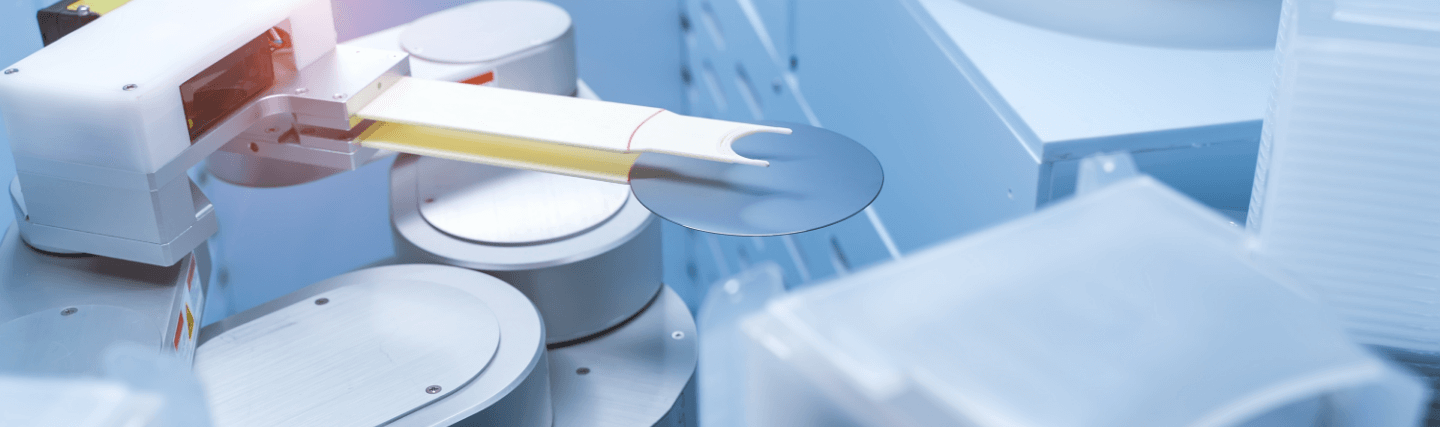
Our Ultra ECP product line does it all, from dual-damascene and through-silicon vias (TSVs) in front-end wafer fab processes to interconnect metal plating used in wafer-level packaging and compound semiconductor manufacturing. Our patented electrochemical plating technologies include multizone anodes for superior uniformity control, rubber-seal plating chucks for superior sealing, partial pulse plating for pattern structure filling, vacuum pre-wetting of wafers, and paddle technologies.
Supplemental Electrochemical Plating (ECP) Technical Resources:
White Paper: Highly Uniform Cu Film Deposition by Electrochemical Methods
White Paper: Optimization of Film Uniformity by Electrochemical Copper Deposition Chamber Design
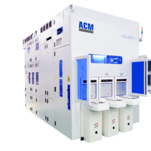
Plating System — Ultra ECP map
Learn More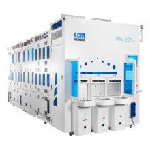
Plating System—Ultra ECP 3d
Learn More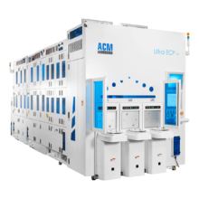
Plating Systems—Ultra ECP ap
Learn More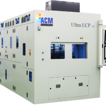
Plating Systems—Ultra ECP G-III
Learn More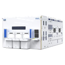
Panel Level Packaging—Ultra ECP ap-p
Learn MoreElectrochemical Plating FAQ

Contact Us
Looking for customized solutions for your Electrochemical Plating (ECP) applications?