Tools and Processes
Discover ACM’s Semiconductor Tools and Processes
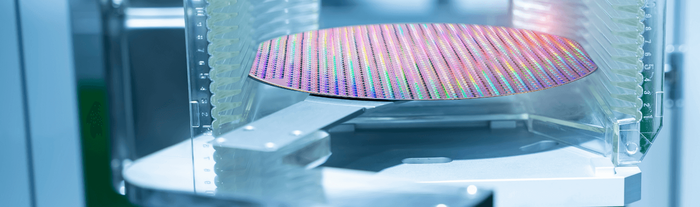
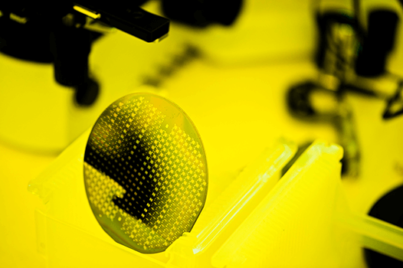
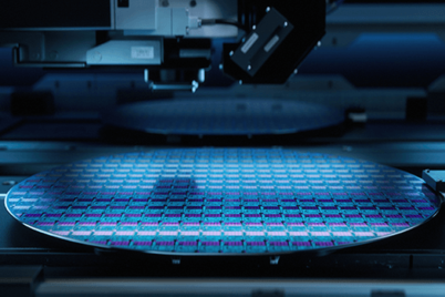
At ACM Research, you’ll find the most advanced semiconductor processing systems available for a host of single or batch wafer processes including cleans, etch, strip, and metal lift-off, as well as electroplating, stress-free polishing, and thermal processes. Our tools are customized to meet your needs, from current and future technology nodes to advance wafer-level packaging and compound semiconductor applications.
Wet Processing
When you’re building advanced microelectronics to meet today’s power, performance, and cost requirements, you need high-performance wet processes that deliver contaminant-free, high-yielding, reliable devices. Our proprietary processes for cleans, surface preparation, etch, photoresist strip, coating, developing, and more will take you there.
Electrochemical Plating
Are you looking for electrochemical plating (ECP) systems that span the spectrum of semiconductor manufacturing plating needs? Our Ultra ECP product line does it all, from dual damascene and through-silicon vias (TSVs) in the front end to interconnect metal plating used in wafer-level packaging and compound semiconductor manufacturing.
Thermal Deposition Processes
At ACM, we also offer 300mm batch processing tools to address your dry processing challenges of low-pressure chemical vapor deposition (LPCVD), atomic layer deposition (ALD), oxidation, and annealing. We designed our furnace systems from the ground up to meet best-in-class requirements.
Track Systems
Are you ready to improve the results of your i-line, KrF, and ArF lithography processes? Then it’s time to consider a lithography track system. Track systems allow you to streamline the coating and developing steps by performing them sequentially on one tool, resulting in increased throughput and improved yields at a low cost of ownership.
PECVD
You know mature node logic and memory devices are more in demand than ever. We think legacy node device manufacturing deserves best-in-class tools and processes. Our PECVD process tools are designed to meet your thick- and thin-film deposition needs. If you need very thin layers or fast process steps, we’ve got a system for that. If you need thicker films and longer process times, we deliver. All while optimizing throughput.
Stress-free Polishing
Chemical mechanical planarization (CMP) alone is no longer enough to address your yield issues associated with TSV and FOWLP processes. That’s why we developed our proprietary stress-free polishing (SFP) technology. As the perfect complement to CMP, it electrically removes metal ions from the wafer surface.

Contact Us
We look forward to providing customized solutions for your wet wafer processing, ECP, Furnace, Track, PECVD, and SFP applications.