Semiconductor Manufacturing
Discover How We Support IC Manufacturing
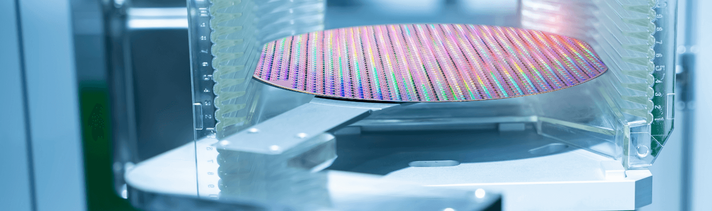
To accommodate the requirements of digital devices, you’re developing progressively faster, more powerful, smaller, and lower-cost semiconductors chips. You need process tools that help you achieve the finest feature geometries while also preventing the “killer defects” that reduce yields and, therefore, profit. At ACM Research, we’ve got the tools to support you.
Proprietary Cleaning and Deposition Processes
As logic and memory device technology nodes continue to shrink, we continually innovate proprietary solutions to address both your legacy and advanced technology requirements.
- Smart Megasonix™ combines jet spray with transient cavitation to gently remove stubborn particles from fragile IC circuitry
- Space Alternated Phase Shift (SAPS™) technology uses megasonic waves to remove random defects from flat and patterned wafers
- Timely Energized Bubble Oscillation (TEBO™) provides efficient, damage-free cleaning for both conventional 2D and 3D patterned wafers at advanced process nodes
- The Multi-Anode Partial Plating function in our ECP systems successfully deposits metal layers on dual damascene structures or through silicon vias
- Our Ultra Furnace platform addresses dry processing challenges of low-pressure chemical vapor deposition (LPCVD), atomic layer deposition (ALD), oxidation, and annealing
The bottom line: Our systems remove the tiniest particles and most stubborn residue and deposit ultra-thin, full-coverage films. They are designed to eliminate and prevent potential causes of defects from any wafer surface, regardless of topography.
PECVD Systems – PECVD SiCN
Learn More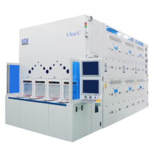
Cleaning Systems—Ultra C SAPS
Learn More
Cleaning Systems—Ultra C TEBO
Learn More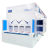
Cleaning Systems—Ultra C Tahoe
Learn More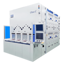
Cleaning Systems—Single Hot SPM
Learn MoreCleaning Systems—Bevel ETCH
Learn More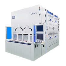
Cleaning Systems—Ultra C b
Learn More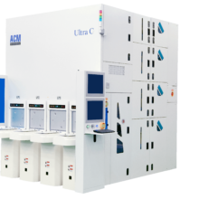
Scrubber Systems—Ultra C s
Learn More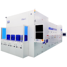
Cleaning Systems—Ultra C wb
Learn More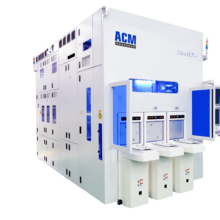
Plating System — Ultra ECP map
Learn More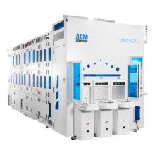
Plating System—Ultra ECP 3d
Learn More
Furnace Systems—Ultra Fn
Learn More
Furnace Systems—Ultra FnA
Learn MoreFurnace Systems—Ultra FN Atmospheric Pressure Oxidation/Anneal
Learn More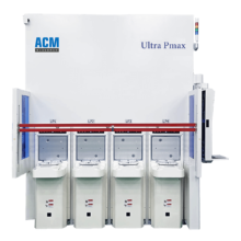
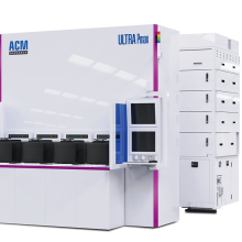
PECVD Systems—Ultra Pmax™
Learn More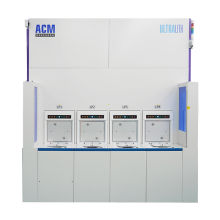
Track Systems—Ultra Lith Track
Learn More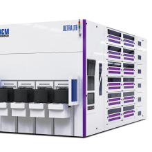
Track Systems – Ultra Lith KrF
Learn More
Contact Us
We look forward to providing customized solutions for your wet wafer processing, ECP, Furnace, Track, PECVD, and SFP applications.