
June 11, 2026 ~ Wafer cleaning is one of the most critical steps in the semiconductor process flow, especially as dimensions continue to shrink to below the 1-nanometer (nm) node. Photoresist residue and particulates can reduce yields in large-die AI chips, impacting the performance of the final product or causing the chips to be scrapped. The sulfuric acid hydrogen peroxide step, or sulfuric peroxide mixture (SPM), is essential for removing organic contaminants from post-etch substrates and ion-implanted films, as well as for platinum silicide residue removal. SPM processes traditionally have been performed in tanks […] Read More

Blogs and Articles

May 18, 2026 ~ Following the launch of our ACM Planetary Family™, which brings together a process-aligned portfolio for semiconductor manufacturing, we delve deeper here into each of the planet series and how they reflect our product lines. Our offerings are grouped into eight different series that represent the essential stages in front-end and advanced packaging, providing a clearer path to identifying the right solutions for specific needs. With this approach, customers can more easily find the […] Read More

May 6, 2026 ~ As the feature sizes and critical dimensions of logic, memory and analog semiconductor devices shrink with advanced technology nodes, the sensitivity to submicron contaminants has increased significantly. Consequently, the use of wet cleaning technology to remove particulates and contaminants is critical to the success of semiconductor manufacturers. Single-wafer and batch cleaning technologies are both used […] Read More
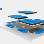
April 3, 2026 ~ One of the most important shifts in semiconductor manufacturing today is not just the continued growth of wafer-level packaging (WLP), but the increasing reliance on enabling, highly specialized process technologies. As device architectures evolve toward heterogeneous integration (HI) and chiplet-based designs, key technologies such as wet processing, electrochemical plating (ECP), plasma-enhanced chemical vapor deposition (PECVD), […] Read More

February 17, 2026 ~ Silicon carbide (SiC) and gallium nitride (GaN) are becoming mainstream within the semiconductor industry due to material properties that make them ideal for multiple applications. These properties—ranging from high thermal conductivity and mechanical strength to optical refractive index control—have made SiC and GaN suitable candidates for multiple end products. Some key applications include power and […] Read More

December 15, 2025 ~ As 2025 comes to a close, ACM Research reflects on a year of advanced packaging innovations, global collaboration, and industry recognition. From wafer-level packaging (WLP) to panel-level packaging (PLP), our team has expanded the capabilities of semiconductor manufacturing tools while connecting with customers and partners across the globe to deliver solutions that drive real-world impact. […] Read More
November 24, 2025 ~ ACM Research was honored to receive a 2025 Global Technology Award in the category of Cleaning Equipment for its Ultra C vac-p flux cleaning tool. Presented annually by Global SMT & Packaging, the awards recognize top-performing and trailblazing solutions addressing the electronics manufacturing industry’s most critical challenges. The award was presented during a ceremony at […] Read More
November 13, 2025 ~ Challenges with Conventional Chemical Mechanical Polishing As logic device dimensions continue to shrink, new interconnect materials are required to maintain electrical performance and long-term reliability. Ruthenium (Ru) has emerged as a strong candidate for advanced logic applications, including high-performance computing (HPC) and artificial intelligence (AI). With its superior electrical characteristics and lower diffusion tendency compared […] Read More
October 20, 2025 ~ ACM Research was named the 2025 Innovator of the Year by the Portland Business Journal, receiving the top honor in the publication’s annual Oregon Makers & Manufacturing Awards. Each year, the Portland Business Journal recognizes manufacturers driving the regional economy through innovation, excellence, and productivity. The Innovator of the Year award specifically highlights one company […] Read More
August 18, 2025 ~ Plasma-enhanced chemical vapor deposition (PECVD) has been a critical part of the semiconductor manufacturing process since the 1980s. With chipsets designed for AI applications transitioning from wire bonding to 2.5 and 3D packaging, PECVD processes have rapidly gained importance within the heterogeneous manufacturing process. PECVD enables the deposition of high-quality dielectric films for 3D packaging […] Read More