
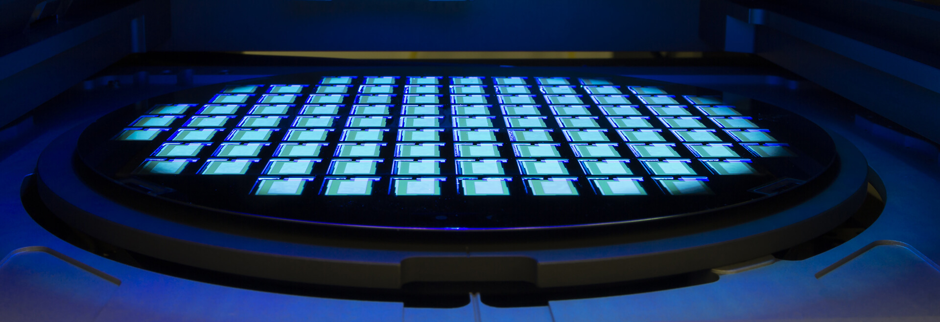
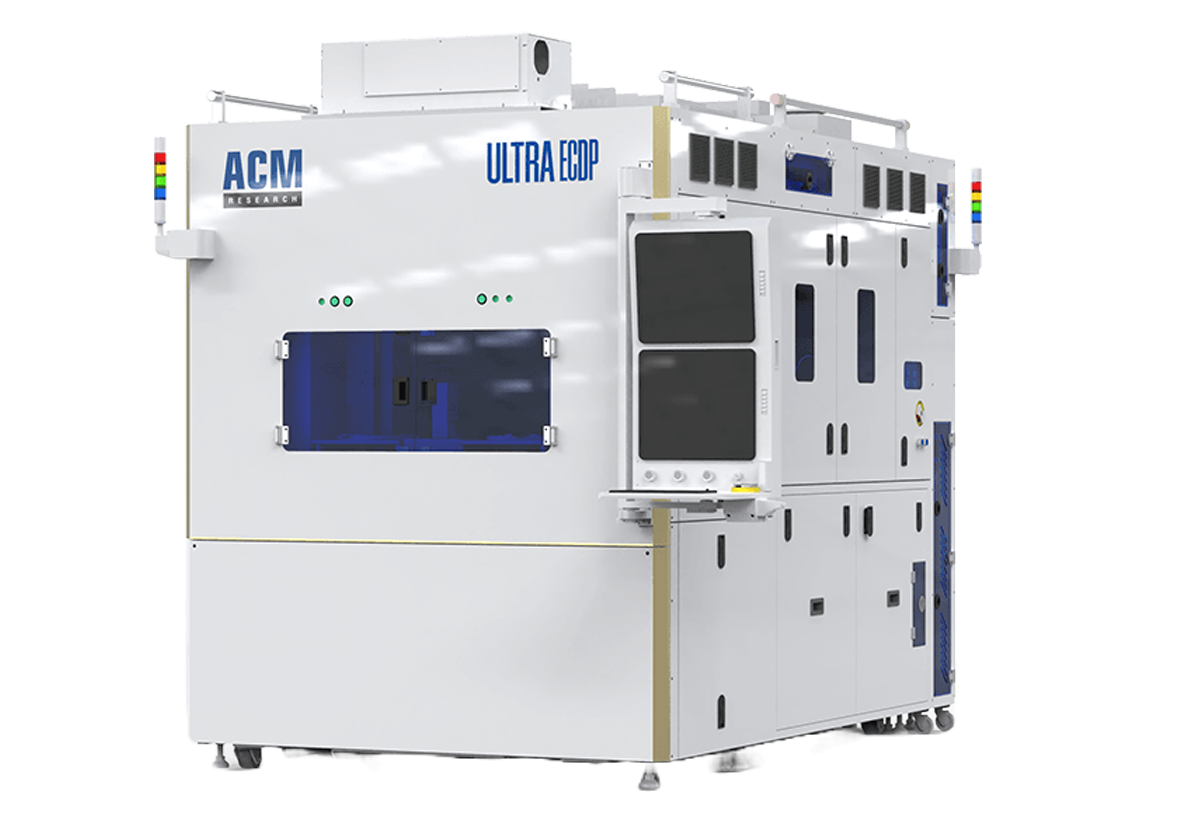
Deplating System – Ultra ECDP
For wide-bandgap compound semiconductor applications
The Ultra Electrochemical Deplating (Ultra ECDP) tool is specifically designed for emerging wide-bandgap compound semiconductor manufacturing. It supports specialized processes including Au bump removal, thin-film Au stripping and etching, and deep-hole Au removal, with integrated pre-wet and cleaning chambers for complete process control. The system features precise chemistry circulation and advanced multi-anode electrochemical deplating technology, enabling reduced side etching, excellent surface finish and high uniformity across all features. Typical performance includes <5% (3 sigma) uniformity, undercut of less than 1μm and consistent Au line definition.
As the compound semiconductor market continues to grow, Au is emerging as a preferred conductor material for these devices due to its high conductivity, corrosion resistance and malleability. However, it also introduces process challenges in plating and etching. The Ultra ECDP tool is engineered to address these challenges and support the evolving requirements of compound semiconductor manufacturing.
Major Benefits
- Horizontal deplating with no cross-contamination
- Modular platform supports integration of deplating and plating processes within a single platform
- Multi-anode technology for controlling deplating in different areas
- High-performance Au removal of bumps, thin films and deep holes with industry-leading plating and stripping uniformity
Features & Specifications
- Configurable with 2 open cassettes and 1 vacuum arm
- Compatible with 6-inch and 8-inch platforms
- Wafer sizes: 150mm, 159mm, 200mm
- Configurable pre-wet chamber, clean chamber and up to 4 deplating chambers (DeAu)
- Process performance:
- Within-wafer uniformity: <5% (3 sigma)
- Wafer-to-wafer uniformity: <3%
- Undercut: <1µm

Contact Us
Looking for customized solutions for your wet wafer processing, ECP, Furnace, Track and SFP?