
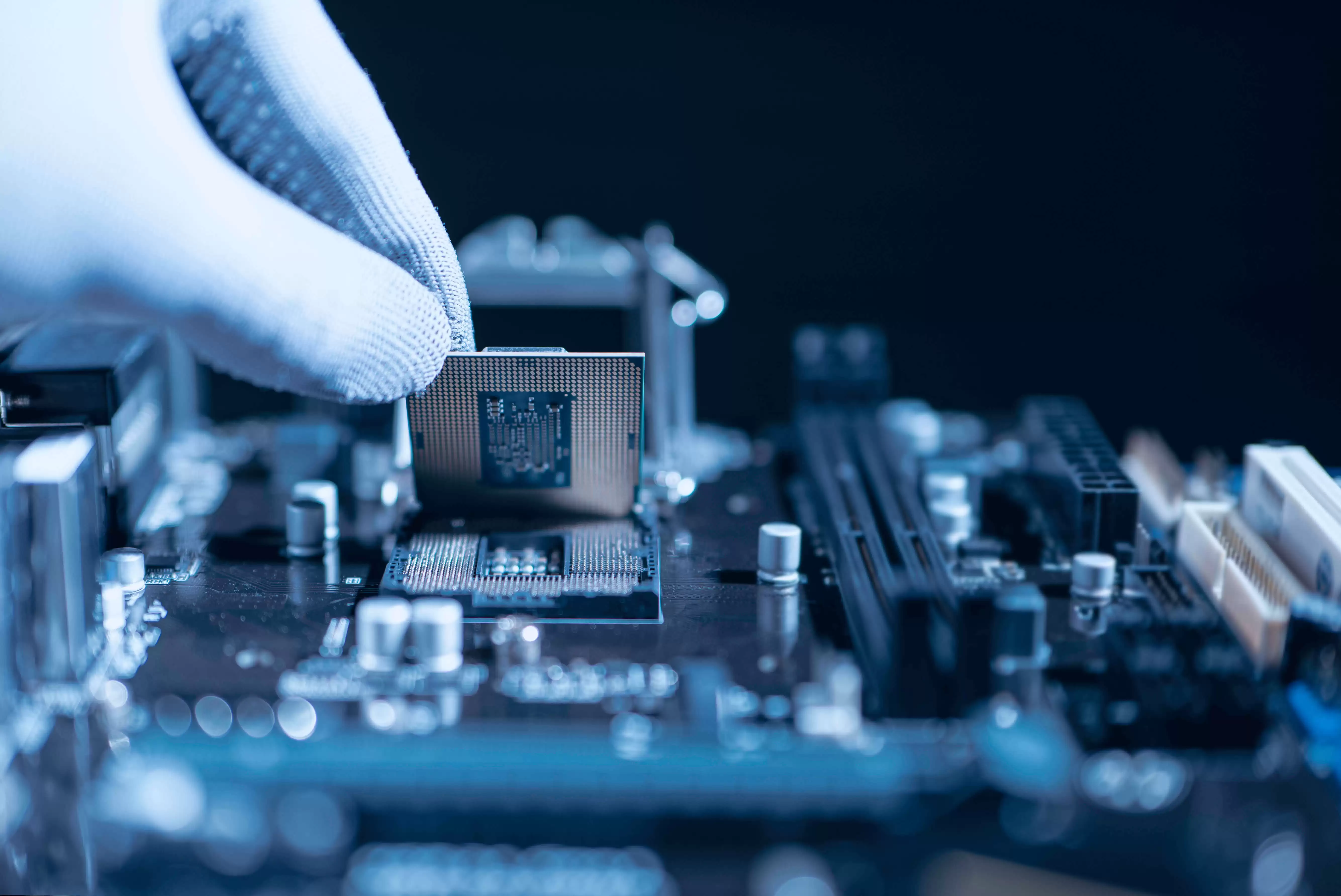
High-performance computing has been reshaping the semiconductor industry for more than a decade. The explosive growth of computing power needed for artificial intelligence (AI) has been driving hyperscale data centers, which in turn, have been driving the need for high-performance semiconductor systems. The concept of packaging logic chiplets with high bandwidth memory (HBM) into multi-reticle packages is driving a shift from performing packaging processes on round 300mm substrates using fan-out wafer-level packaging (FOWLP) to larger square substrates. A larger number of dice can be processed using FOWLP technology in equipment that has been developed to process larger square substrates, creating fan-out panel level packaging (FOPLP).
These two packaging technologies can be used hand in hand to meet the challenges of multi-reticle 2.5 and 3D packaging. Fan-out packaging has emerged as the packaging technology of choice for 2.5 and 3D packages. It enables compact, high-performance solutions as it improves chip-to-chip communication and can create a thinner packaging form factor, which is vital for many applications.
There are multiple pain points as multi-reticle packaging grows. The first is that by moving to square substrates, one can significantly increase the number of dice that are processed at one time. A 600mm x 600mm panel has approximately more than 5.7x the area of a 300mm round silicon substrate with subsequent improved yield due to placing a square die on a square substrate. AI packages need high electrical performance, which requires ultrafine routing to meet power and performance goals.
Cost is another pain point. As the demand for AI systems increases, manufacturing costs need to be lowered without compromising reliability. As panel level packaging (PLP) scales, precise alignment and placement of redistribution layers (RDL) are critical. Scaling to panels can also lead to uniformity limitations as conventional vertical plating tools struggle with uniformity across large substrates, impacting device yield and performance.
ACMR’s RDL Copper Deposition Capabilities
At ACM Research, we designed and built multiple process tools to support FOWLP and FOPLP. Our Ultra ECP ap system targets wafer-level packaging with an RDL copper fill that enables the extremely fine features used for leading-edge packaging. Our Ultra ECP ap-p system is built upon our robust wafer-level packaging expertise and is designed for the large-scale panel-level packaging market. The system can handle glass carriers up to 600 mm2. The Ultra ECP ap-p builds on the history and excellence of the ECP ap system and provides excellent uniformity, supporting the fine features needed to support the advanced packaging needs of high-performance computing.
The technology of the Ultra ECP tools has been refined over multiple years, with key features that make it the best in class for advanced packaging. The patented horizontal spin plating ensures superior uniformity across wafers and panels, and reduces defects while improving substrate yields compared to vertical plating systems. The adaptive alignment ensures RDL patterns are precisely aligned to die placement and maintains yield as our customers’ packaging scales up production. The Ultra ECP tools can fill copper geometries down to 10 μm and can support the industry’s drive to smaller features — as small as 2 μm lines and spaces. The Ultra ECP tools can also deposit additional metals needed for advanced packaging. In addition to copper, they can perform tin-silver (SnAg) plating for solder, nickel and gold. In addition to multiple metals, the Ultra ECP tools can support both wafers and panels, which enable Outsourced Semiconductor Assembly and Tests (OSAT) and packaging manufacturers to develop processes on wafers and then scale up to panels with only minor reconfiguration of the Ultra ECP tool.
Technology Applications
Our Ultra ECP tools have been industry-proven in many different applications. They have successfully delivered the fine routing needed for high performance in microelectromechanical systems (MEMS) and image sensors. They have successfully supported the complex RDL needs of large-area Graphics Processing Unit (GPU), Central Processing Unit (CPU) and HBM dice. And they have been proven to help lower costs and increase throughput when an advanced packaging customer upgrades from a FOWLP to FOPLP process.
Our portfolio of Ultra ECP tools have a proven history in wafer-level copper damascene and packaging plating, which translates seamlessly to panel-level solutions. The horizontal spin plating and the adaptive alignment are proprietary advantages that differentiate our tools from the competition. The tools are built to meet current demands while future-proofing facilities for the shift toward panel-scale manufacturing, enabling the next phase of advanced semiconductor packaging with industry-leading plating solutions for FOWLP and FOPLP.
Interested in learning how we can help future-proof your advanced packaging production with best-in-class plating technologies? Reach out to our team here.