Panel Level Packaging

Fan-Out Panel Level Packaging (FOPLP) Overview

Wafer-level packaging for 2.5D and 3D packaging technologies is transitioning from fan-out wafer-level packaging (FOWLP) to fan-out panel-level packaging (FOPLP). Moving to FOPLP will help reduce processing bottlenecks and improve cost and packaging yield. ACM Research has applied its expertise in FOWLP technology to develop the first-of-its-kind panel-level processing tool that will enable customers to achieve their panel-level processing goals.

Capable of Multiple Panel Processes

Leveraging the company’s expertise in the packaging cleaning and plating process, ACM Research’s suite of panel-level process tools offers a multitude of capabilities to meet customers’ advanced panel-level processing needs and build the challenging structures for advanced packaging requirements.

  • The Ultra C vac-p Flux provides superior vacuum-based cleaning technology for the removal of contaminants in hard-to-reach spaces, especially in the bumping process.
  • The Ultra ECP ap-p can be used for plating steps in a variety of processes including pillar, bump, and RDL. The panel plating equipment can also be utilized for fan-out and through-glass via (TGV) processes.
  • The Ultra ECP ap-p can support up to 16 plating chambers for copper, nickel, tin-silver, gold, and other plating materials.
  • The Ultra ECP ap-p can handle organic and glass substrates sized 510 x 515 mm2 and 600 x 600 mm2 while effectively managing cover warpages up to 7 mm.
  • The Ultra ECP ap-p provides cost-effective, high-yield FOPLP processing technology.
  • The Ultra C bev-p double-sided bevel etching tool is capable of bevel etch and copper removal for panel-level packaging.

As a leader in FOWLP process equipment, ACM Research can accommodate special process requests and deliver custom-made, differentiated panel-level processing equipment at a competitive price.

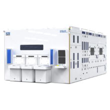
Panel Level Packaging—Ultra ECP ap-p

Learn More
ACMR Ultra C vac-p FOPLP cleaning tool

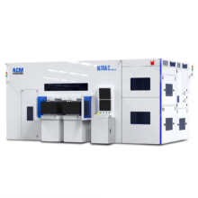
Panel Level Packaging—Ultra C vac-p Flux Cleaning Tool

Learn More
ACMR Ultra C vac-p FOPLP cleaning tool

Panel Level Packaging—Ultra C bev-p tool

Learn More

Both are advanced semiconductor packaging methods. In PLP, chips are assembled on large rectangular panels instead of round wafers, unlike WLP, which is limited to the size of silicon wafers (typically up to 300mm), PLP allows for larger surface areas, increasing productivity and reducing cost per chip. This method supports greater scalability and flexibility in layout for high-volume production.

Fan-out panel-level packaging (FOPLP) offers several advantages over traditional packaging that make it an efficient and scalable solution for next-generation electronic devices. It enables thinner, lighter packages with better thermal and electrical performance, and larger panel sizes let more chips be processed simultaneously—delivering a lower cost per unit. In addition, FOPLP is ideal for high-density applications, as it supports finer line widths and tighter pitches.

Common PLP materials include epoxy molding compounds, photoresists, redistribution layers (RDLs) made of copper, and dielectric materials such as polyimide or epoxy. During processing, substrates often consist of temporary carrier materials such as glass or silicon. For final packaging, however, organic laminate panels are commonly used, as they provide high thermal stability and mechanical strength, and are compatible with fine-line lithography and high-density interconnects (HDI).

The FOPLP process involves several key steps, including wafer fabrication, reconstitution and panelization, redistribution layer (RDL) fabrication, die placement, molding, and final dicing. Die are placed on a carrier and molded into a panel, which is thinned and planarized to prepare for RDL formation. Fine-line metallization and dielectric layering enable high-density interconnects. Finally, the panel is singulated into individual packages. Throughout the process, surface cleaning, wet processing, and stress-free planarization (SFP) are critical for maintaining uniformity and yield.

FOPLP is gaining traction as system integration and miniaturization become more important for a broad range of markets. The process is best suited for applications that demand high performance and compact form factors, including smartphones, tablets, and wearable devices, as well as automotive electronics, 5G infrastructure, and advanced computing applications such as artificial intelligence (AI) and high-performance computing (HPC).

Contact Us

We look forward to providing customized solutions for your wet wafer processing, ECP, Furnace, Track, PECVD, and SFP applications.