Stress-free Polishing
Discover ACM’s Stress-free Polishing Capabilities
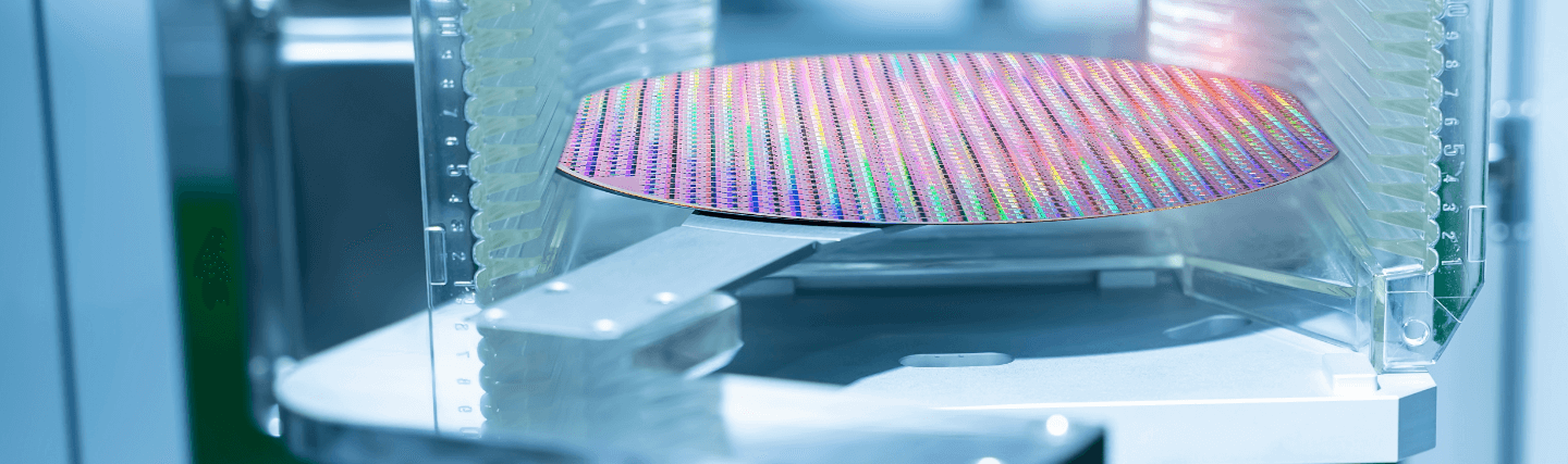
As advanced packaging architectures push the limits of interconnect density and wafer complexity, traditional approaches to copper overburden removal are increasingly challenged. High topography, fragile dielectric layers, and complex structures such as through-silicon vias (TSVs) and fan-out redistribution layers (RDL) demand greater control over surface integrity prior to planarization. Meeting this requirement is the critical role played by stress-free polishing (SFP).
SFP is a pre-chemical-mechanical planarization (CMP) copper overburden removal step designed to minimize mechanical and thermal impact on the wafer surface. Unlike conventional approaches that can introduce subsurface damage, dishing, or non-uniform material removal, SFP focuses on gently reducing excess copper while preserving underlying structures. By lowering stress at this stage, manufacturers can significantly reduce defect formation, including microcracks, delamination, and surface irregularities that often propagate during downstream CMP.
The result of this low-stress, low-damage polishing is a more controlled and predictable planarization process. Having less copper remaining and a more uniform surface profile entering CMP reduces the burden on polishing slurries and pads, improving process stability and extending the life of consumables. Just as importantly, defect reduction at the pre-CMP stage translates directly to higher yield and more consistent device performance.
These benefits are particularly evident in TSV and fan-out packaging, where large copper features and heterogeneous materials amplify the risk of stress-induced damage. Low-damage polishing enables tighter process control across varying feature densities, supporting the uniformity required for high-performance interconnects.
ACM’s SFP approach builds on these principles, delivering a low-stress, low-damage copper overburden removal solution that prepares wafers for more efficient and reliable CMP. By addressing defectivity and surface quality earlier in the process flow, SFP helps enable the next generation of advanced packaging.
Stress-Free Polishing FAQs
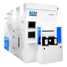
Stress Free Polishing Systems—Ultra SFP
Learn More
Contact Us
We look forward to providing customized solutions for your SFP applications.