
By Sally-Ann Henry and Jim Straus, ACM Research
Let’s face it: When it comes to choosing a substrate material for building power semiconductors, silicon (Si) is no match for up-and-coming compound semiconductors like silicon carbide (SiC) and gallium nitride (GaN). Because of their fundamental material properties, these compound semiconductors can do things that simply aren’t possible with silicon.
Until recently, Si was the most cost-efficient semiconductor material, and it sufficiently met the needs of power semiconductor devices. However, emerging applications like electric and hybrid vehicles (EV/HEV), rapid charging devices for mobile devices and EVs, and the 5G network need power devices that operate at higher frequencies, can handle higher voltages, are more thermally conductive, and can endure a broader range of temperatures.
That’s why manufacturers who want to be on the leading edge of technology are investing in manufacturing devices using compound semiconductors. In fact, analysts predict the global compound semiconductor market to reach $212.9 billion by 2027, registering a CAGR of 11.1% from 2020 to 2027. The SiC market alone is predicted to reach $1.8 billion in that timeframe, and the GaN market is expected to be worth $24.9 billion by 2026.
With that in mind, we thought it might be a good time to brush up on what makes compound semiconductors so special and how to overcome some of the process challenges.
Compound Semiconductors: The Basics
Simply put, compound semiconductors are made from two or more elements, while silicon semiconductors are made from a single element. They are often referred to as “III–V materials,” because most compound semiconductors are created by combining elements from Group III and Group V of the Periodic Table of elements. GaN falls in this category (Figure 1).
Others are made from Groups II and VI (cadmium telluride [CdTe], zinc selenide [ZnSe], and others). SiC is made from elements within the same group (IV).
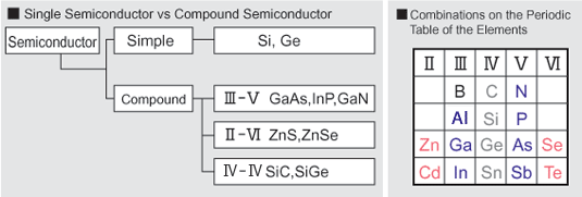
Figure 1: Single Semiconductor vs. Compound Semiconductor. Source: Sumitomo Electric
In recent years, the cost of manufacturing compound semiconductors has declined. While it’s still much higher than the cost of silicon semiconductors, the special properties of these elements have become more important for today’s emerging applications in the automotive, telecommunications, and consumer markets. When compared with Si, both SiC and GaN exhibit:
• Higher frequency and bandgap
• Better electrical breakdown field
• Better thermal conductivity
• Higher temperature endurance and a wider temperature operation range
Si vs. SiC vs. GaN
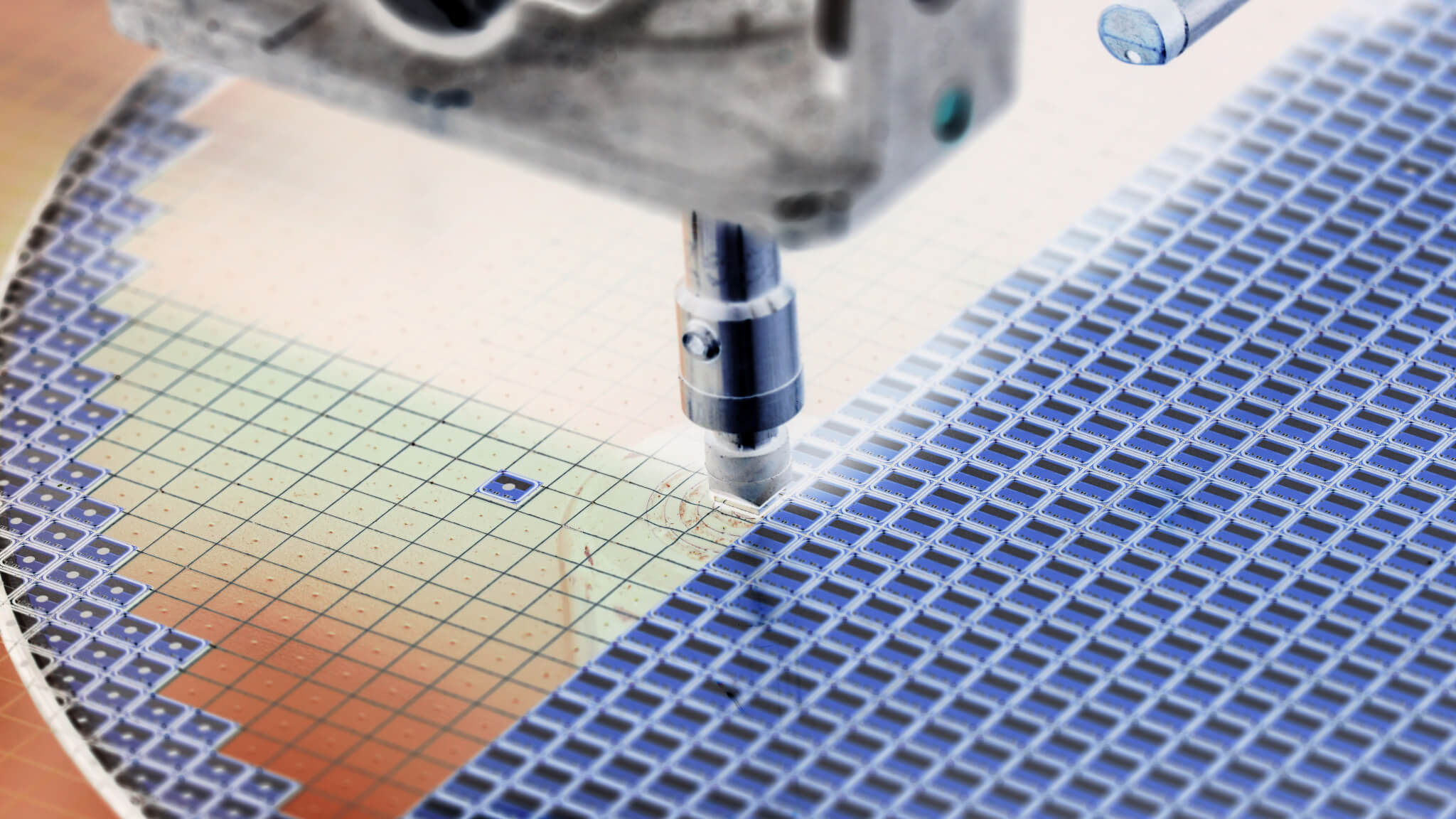
Like Si, SiC is grown in ingot form before being sliced into wafers. However, while Si ingots can grow in one to five minutes, it can take three to four weeks to grow a SiC ingot. That’s why SiC costs more to manufacture than Si. However, through technology innovation, that’s being reduced to one to two weeks. Unlike Si and SiC, GaN is not grown in ingots. The wafers are formed by depositing a thin film on a silicon wafer.
Both SiC and GaN devices are available on 4- and 6-inch wafers. To increase yields to meet growing demand for these compound semiconductor materials, some companies are developing 8-inch wafer capabilities.
While SiC and GaN offer some of the same advantages over Si, SiC is more complex to manufacture. Because SiC withstands higher temperatures and has a wider bandgap than GaN, devices built from it can handle having 800 volts run through them. For this reason, Tesla chose SiC over GaN for its network of EV charging stations.
SiC Process Challenges
Despite the overall performance advantages, processing SiC device wafers poses some challenges that manufacturers don’t face when working with Si. For example, SiC wafers are transparent, which makes handling, marking, and metrology challenging. Wafer thickness and tendency to bow create challenges for maintaining flatness. They require thick metal deposition and extremely high temperatures (1800°C) for annealing. Lastly, there is no perfect design.
Optimizing Processes Using ACM Research’s Tools
Figure 2 provides an overview of the SiC process flow. The process chemistries used in SiC device manufacturing are like those used for standard integrated circuits. As such, for certain processes, the same toolsets used in Si wafer processing can be used, including:
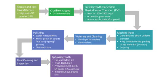
Figure 2: SiC Wafer Manufacturing Process Flow. Source: National Renewable Energy Laboratory
• Electrochemical plating
• Selective wet etch
• Post chemical mechanical planarization (CMP) cleaner
• Metal lift-off
At ACM Research, we recognize the growing demand for compound semiconductors and consistently think of ways to optimize these process steps for our customers. Additionally, our most advanced processes are available on tools that can handle wafer sizes up to 200mm.
For example, our Smart Megasonix™ cleaning systems with patented space alternate phase shift (SAPS™) technology are ideal for SiC post-CMP cleaning. SAPS wet clean modules can be integrated directly into a CMP tool to keep SiC wafers in a clean environment throughout the CMP process, preventing them from being dried before completion of the process. Wafers go into the tool wet and come out dry, ready for the next process step. ACM can also offer multi chamber wet etching tools, as well as metal lift off capabilities, in the combined batch and single wafer tool. In addition, we have the electrochemical plating (ECP) for depositing different metal films such as Silver (Ag) and Nickel (Ni).
We are excited about the promise that compound semiconductors pose for the future of power devices. Contact us to learn how ACM Research can support your SiC process needs.