Thermal Deposition Processing
Discover ACM’s Thermal Processing Capabilities
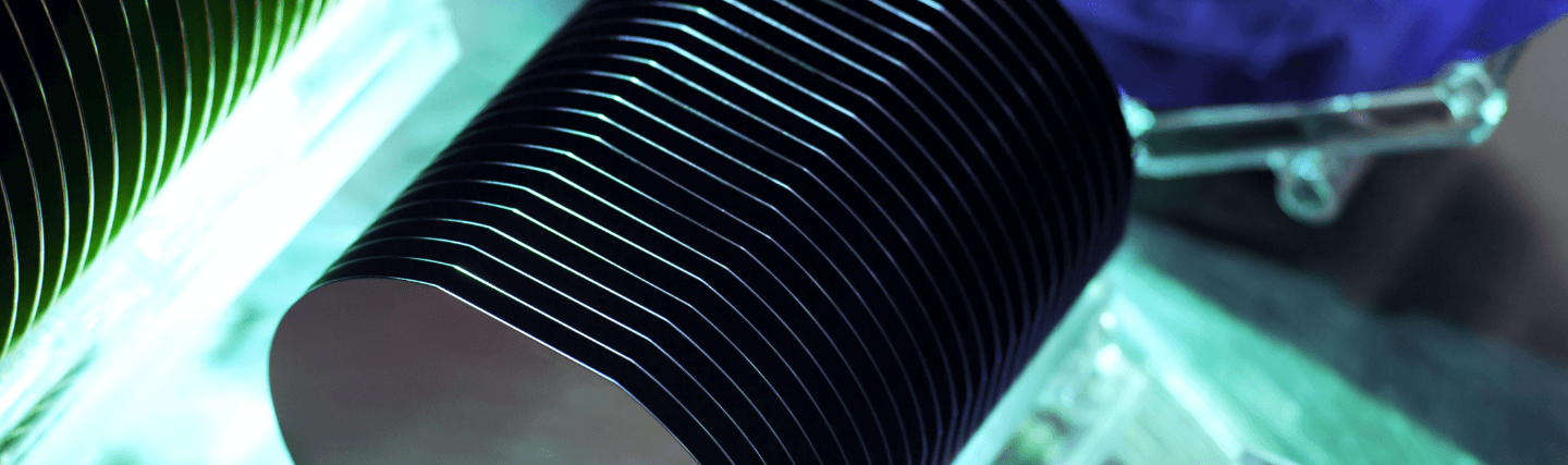
As semiconductor technology nodes shrink, you’re probably noticing that the complex, fine geometries make it increasingly challenging to reliably deposit thin silicon oxide or nitride films. Providing consistent and stable heat control is paramount in maintaining wafer integrity. Not just any furnace system will do. At ACM Research, we’ve got you covered.
Does Your Furnace Heater Measure Up?
At ACM, we’re not all wet. We also offer 300mm batch processing tools to address your dry processing challenges of atmospheric pressure chemical vapor deposition (APCVD) low-pressure chemical vapor deposition (LPCVD) and atomic layer deposition (ALD). But that’s not all—our configurable systems also support un-doped poly deposition, doped poly deposition, gate oxide deposition, high-temperature oxidation, and high-temperature annealing.
We designed the Ultra Furnace System from the ground up to meet best-in-class requirements. Its innovative design combines ACM’s proven software technology with new hardware that improves durability and reliability, as well as ACM’s process-control IP that uses a proprietary control algorithm to deliver stable control of temperature, pressure, and gas flow rate.

Furnace Systems—Ultra Fn
Learn More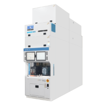
Furnace Systems—Ultra FnA
Learn MoreFurnace Systems—Ultra FN Atmospheric Pressure Oxidation/Anneal
Learn MoreThermal Deposition Processing FAQ

Contact Us
Looking for customized solutions for your thermal deposition processing?