
While heterogeneous integration of multiple components and 2.5D/3D packaging techniques pair perfectly with complex stacking architectures, these technologies elicit high demands on device manufacturing processes. Through-silicon via is the key enabler, allowing direct chip-to-chip connection through the chip stack without requiring wire bonding or edge wiring.
The growing demand for miniaturized semiconductor chips and their applications in different sectors such as telecommunications, automotive, aerospace and defense, and consumer electronic devices, etc., is accelerating the growth of TSV technology market globally. TSV technology allows state-of-the-art packages to increase packaging density and deliver high-performance and low-power consumption.
However, the optimization of TSV process relies on a broad set of technologies. This information series provides insight into ACM Research’s propriety solutions, illustrating its role and importance to TSV processing and explaining the benefits. First, the focus is on cleaning for TSV process using ACM Research’s SAPS™ megasonic technology.
TSV Process Overview
Before delving into TSV cleaning, it’s important to understand what is involved in the TSV process (see Figure 1) including the cleaning challenges it creates. Typically, the TSV goes through the etching process through the silicon substrate to create cavities, and then fill them with a conductive material, such as copper or tungsten, to form a vertical electrical connection.
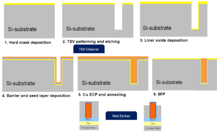
Figure 1. Overview of Through Silicon Via (TSV) process steps
The required TSV size depends on the application. The reactive ion etching (RIE) process, such as Bosch process, is commonly used to fabricate deep vias due to its ability to produce features with vertical sidewalls and high aspect ratio. However, forming these vias with smooth sidewalls is challenged, and the RIE process typically results in the formation of numerous polymer residuals at the bottom and sidewall of vias.
Removing these fluorocarbon polymers and optimizing the TSV requires a reliable cleaning process, after which the via is filled – typically with copper – to make the interconnect between different layers in the 3D stack. This is achieved by electrochemical plating (ECP), followed by the last of these steps, polishing. ACM Research’s proprietary stress-free polishing (SFP) technology affords some unique advantages over other polishing offerings, which will be addressed in part three of this series.
SAPS megasonics
Megasonic cleaning uses sound waves traveling through liquid, producing cavitation – rapid formation and collapse of vapor bubbles within the liquid. Megasonic cleaning’s high-frequency sound waves result in controlled cavitation that gently removes sidewall polymers and residue. By creating a much thinner boundary layer, megasonic cleaning makes chemicals less viscous, enabling them to reach the bottom of vias. This is vital, as incomplete cleaning deteriorates device performance. Particles and residue left in the holes result in low breakdown voltage, high leakage current, and low yield.
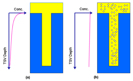
Figure 2. Compared to non-megasonic cleaning (a) chemical concentration in solution reduces with TSV depth at no megasonic effect (b) enhances mass transfer rate and improves the efficiency of residue removal during cleaning.
ACM Research’s Space Alternated Phase Shift (SAPS™) technology takes megasonics a step further, outperforming conventional megasonic cleaning products and exceeding expectations beyond removing random defects (see Figure 2). Unlike the stationary megasonic transducers used in previous generations of megasonic wafer cleaning systems, SAPS technology moves or tilts the transducer while the wafer rotates, enabling megasonic energy to be delivered uniformly across all points on the wafer, regardless of wafer flatness or uniformity.
On a microscopic level, megasonic energy can reach every point on the wafer surface, removing random defects much more effectively and completely than conventional megasonic or jet spray processes. SAPS technology provides uniform megasonic energy distribution to the wafer surface and demonstrates a clear capability for removing residue at the bottom of vias, as shown in Figure 3.
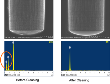
Figure 3. Before cleaning, fluoropolymer residue at the TSV bottom is clearly visible in the SEM image at left, with the x-ray spectra below showing carbon and fluorine signature. Following the SAPS megasonic clean, at right, the SEM shows a clean TSV bottom, with no carbon or fluorine.
The results show that SAPS megasonic technology delivers high cleaning efficiency for fluoropolymer sidewall residue removal in post-silicon-etch TSV cleaning processes, yielding minimal damage to the structures and low material loss.
Now that you have formed TSVs and cleaned them efficiently, these need to be plated using a metal appropriate to the device application. ACM Research’s ECP technology helps ensure your final product’s desired quality and electrical performance.