
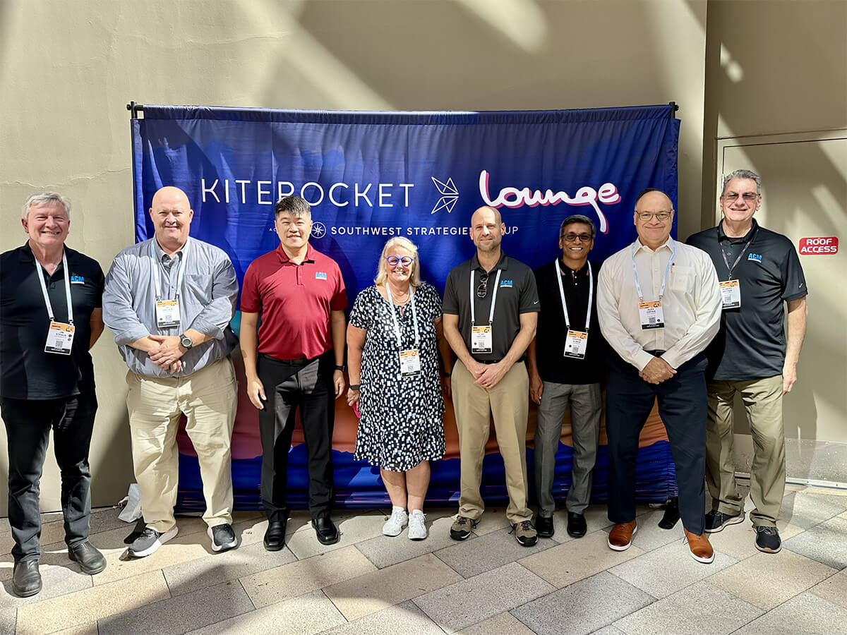
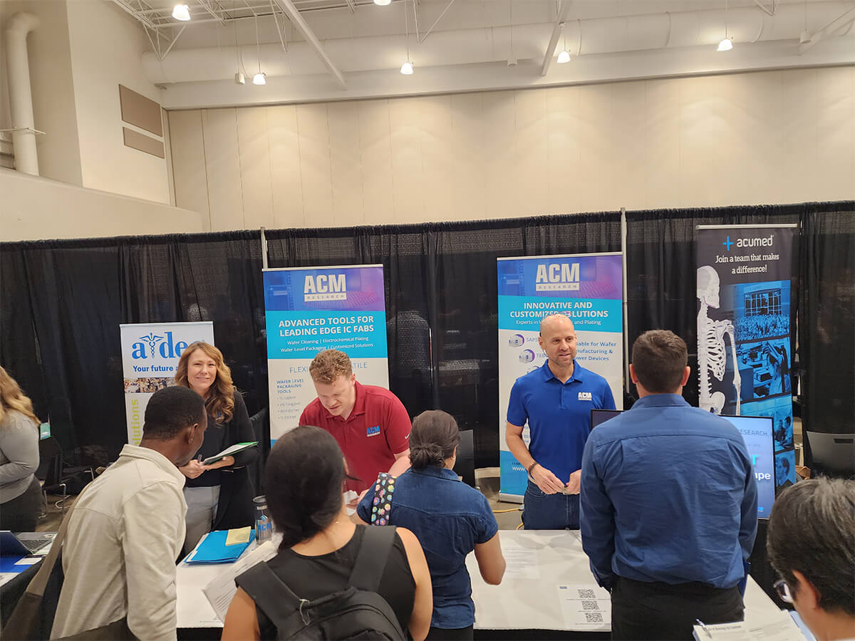
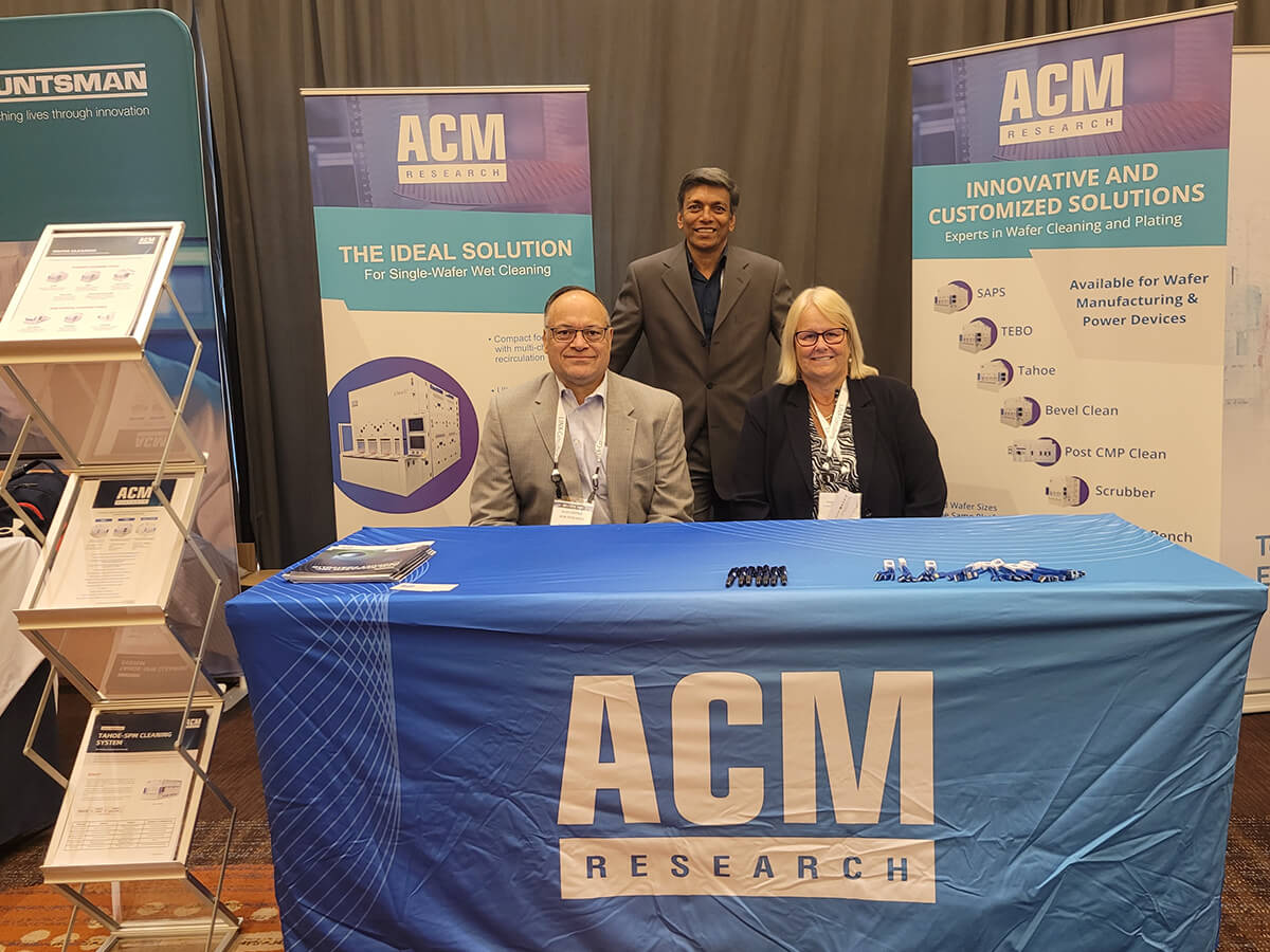
As 2025 comes to a close, ACM Research reflects on a year of advanced packaging innovations, global collaboration, and industry recognition. From wafer-level packaging (WLP) to panel-level packaging (PLP), our team has expanded the capabilities of semiconductor manufacturing tools while connecting with customers and partners across the globe to deliver solutions that drive real-world impact.
Product Launches & Upgrades in Semiconductor Manufacturing
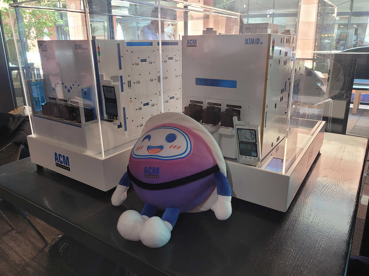
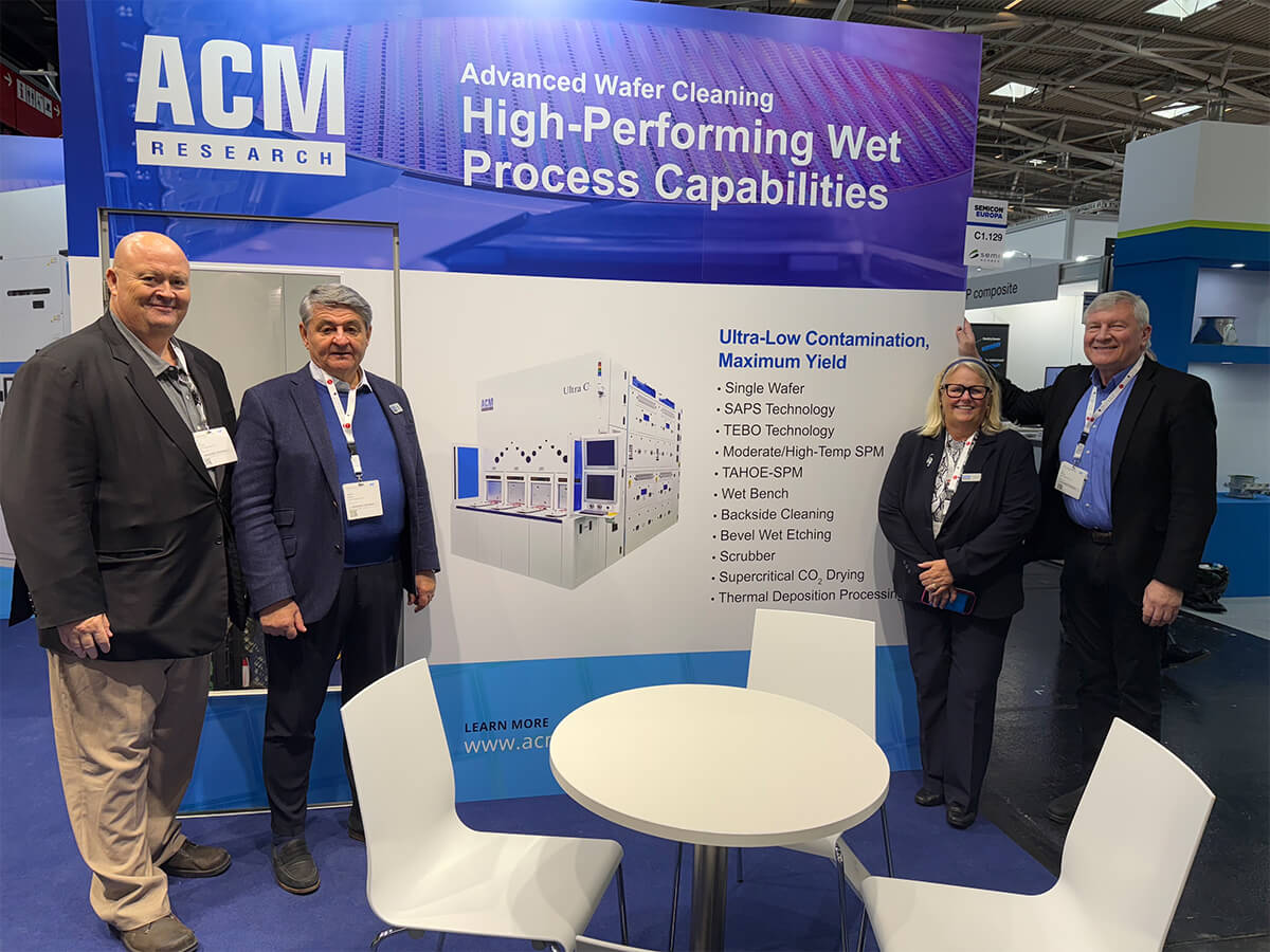
While continuing to build and support our existing products, we grew our vast portfolio of wafer and panel semiconductor manufacturing tools, with upgrades to our existing tools and the addition of new system offerings that address the booming advanced packaging market.
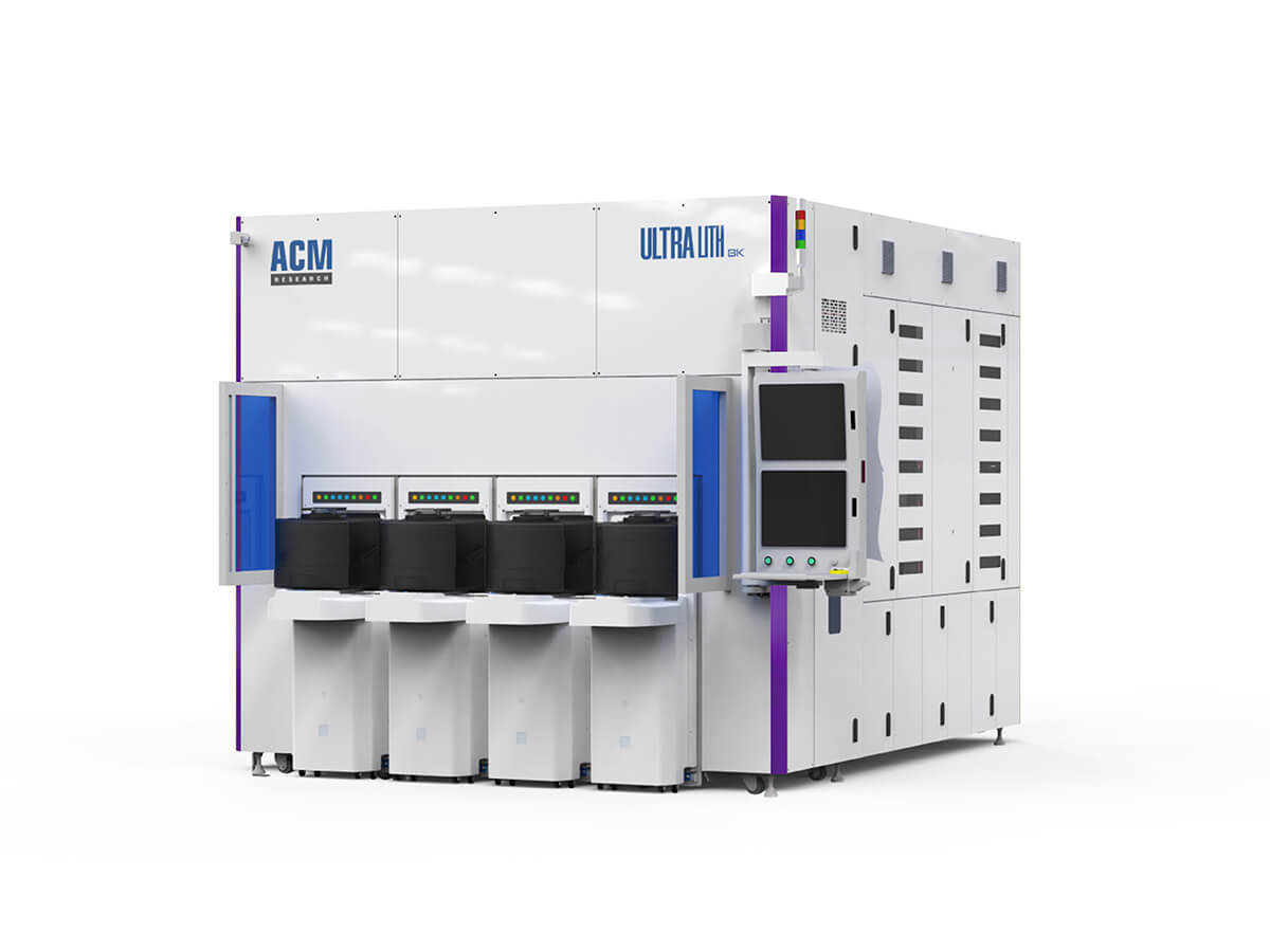
- Ultra Lith BK Photoresist Hardening Tool: Delivered the first system, providing industry-leading UV curing and temperature uniformity.
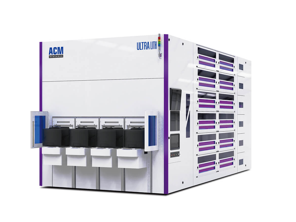
- Ultra Lith KrF Track System: Successfully launched and delivered to a leading logic wafer manufacturer.
- Ultra ECDP Electrochemical Deplating Tool: Designed for wide bandgap compound semiconductor manufacturing, offering superior uniformity and minimized undercut for high-precision gold etch processes.
- Ultra C wb Wet Bench Cleaning Tool: Upgraded with a patent-pending nitrogen bubbling technology for advanced chip manufacturing.
Our continuous focus on innovation and collaboration with customers also led to key milestones, including the qualification of our Single-Wafer High-Temperature Sulfuric Peroxide Mixture (SPM) tool by a major logic device manufacturer, and delivery of our first Ultra ECP ap-p horizontal electroplating tool, strengthening our leadership in fan-out panel-level packaging (FOPLP).
Industry Recognition & Awards in Advanced Packaging
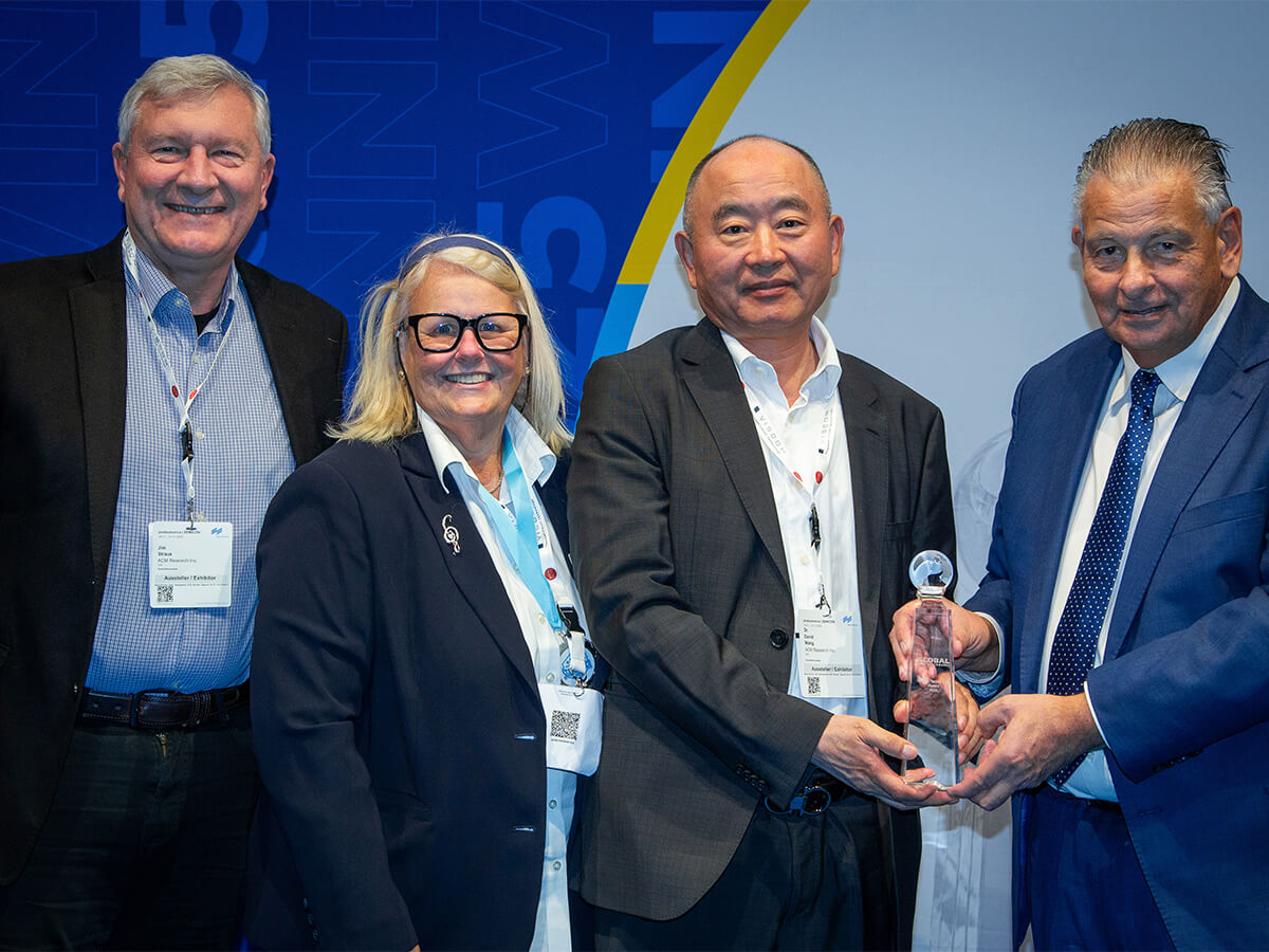
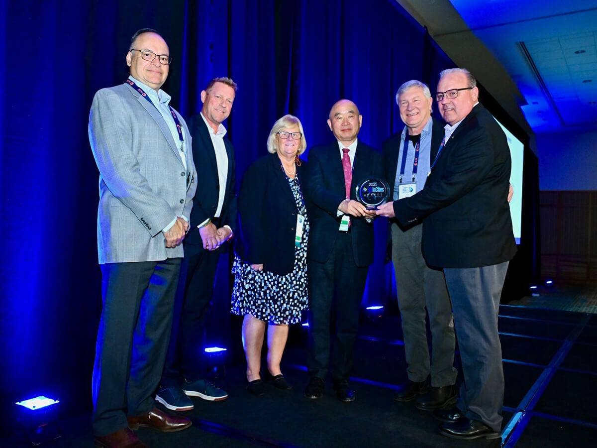
Over the course of the year, our technology and innovations were recognized with several awards. Announced at the IMAPS Device Packaging Conference, our Ultra ECP ap-p tool, designed for FOPLP, won the 3D InCites Technology Enablement award. The award honors companies that have identified and solved critical challenges in the advancement of the heterogeneous integration roadmap, driving the industry forward through cutting-edge solutions and advancements. This award recognition validates our dedication to innovation in addressing customers’ challenges in PLP.
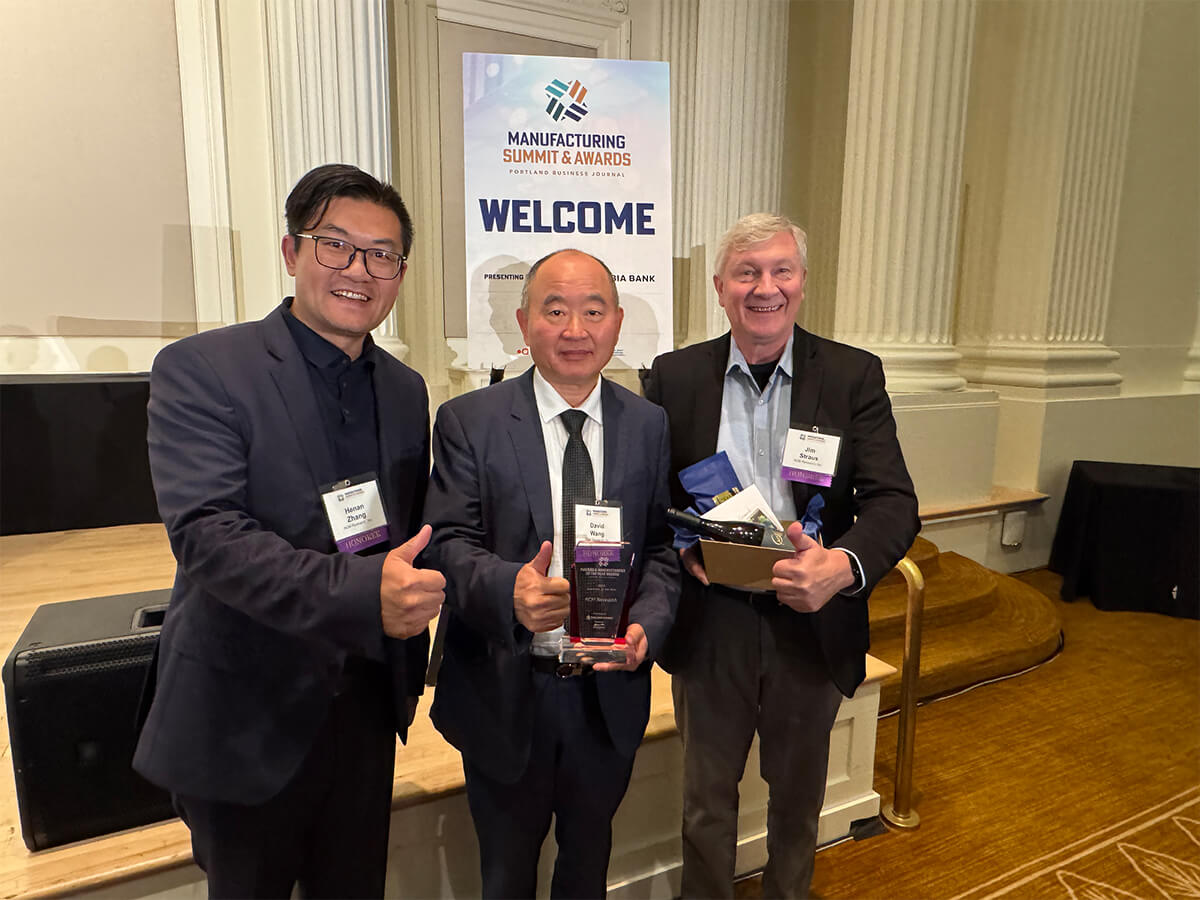
The Portland Business Journal Oregon Makers and Manufacturing Awards named ACM Research as the 2025 Innovator of the Year. Each year, the Portland Business Journal recognizes manufacturers driving the regional economy through innovation, excellence, and productivity. The Innovator of the Year award specifically highlights one company whose breakthrough advancements are transforming its industry. It was a tremendous honor to be recognized as a company representing the strength and ingenuity driving Oregon’s manufacturing sector and the region’s long-term economic growth.
Our team also took home the Global SMT and Packaging award in the category of cleaning equipment. Our Ultra C vac-p flux cleaning tool was recognized as a top-performing and trailblazing solution, addressing one of the most challenging steps in advanced packaging: flux residue removal before underfilling. Engineered on ACM’s proven wafer-cleaning platforms for FOWLP and high-bandwidth memory (HBM), the Ultra C vac-p allows manufacturers transitioning to FOPLP to reduce costs and improve yield performance.
Looking Ahead: Wafer- and Panel-Level Packaging Trends in 2026
As we finish off the year strong, we also look forward to the year ahead with great enthusiasm. With our diverse product offerings, we are well-positioned to play a leading role in WLP and PLP.
As the demand for large chiplets, high-performance graphics processing units and high-density high-bandwidth memory continues to grow, we anticipate an even stronger push for advanced packaging as a necessary element fueling innovation next year. AI and HBM workloads will continue to drive device sizes, interconnect density, and power budgets, driving an accelerated move from traditional wafer-based processes toward glass substrates and 3D stacking.
WLP will keep growing as the production standard for 3D integration, headlined by its use in AI and HBM devices on 300mm wafers using silicon interposers. At the same time, PLP has emerged as a key solution for reducing costs and improving efficiency. According to Yole’s 2025 PLP report, the PLP market is projected to reach $600 million by 2030.
Through the delivery of significant cost savings and achieving substrate utilization beyond 80%, high-end FOPLP and 2.5D interposer technologies are projected to drive AI, HPC, mobile, and high-end consumer markets. Additionally, the evolution from round wafers to square glass panels will allow for more dies per substrate, higher throughput, and better economics for increasingly complex packages.
However, this transition will also come with its own set of challenges as panel sizes will adapt from roughly 310 x 310mm to 600 x 600mm and beyond. It is expected that the lack of standardization will raise both R&D and capital costs for OSATs, fabs, and equipment vendors. Therefore, the development of tools that can handle various glass panel sizes while maintaining uniform process performance and integrating into evolving production flows will be critical in 2026.
As we bring in the new year, ACM Research remains committed to collaborating with customers to solve IC and compound semiconductor manufacturing challenges. By delivering differentiated, high-performance packaging solutions, we aim to not only support the mainstream manufacturing adoption of PLP, but also drive the next wave of innovation, efficiency, and scale in the semiconductor industry.