
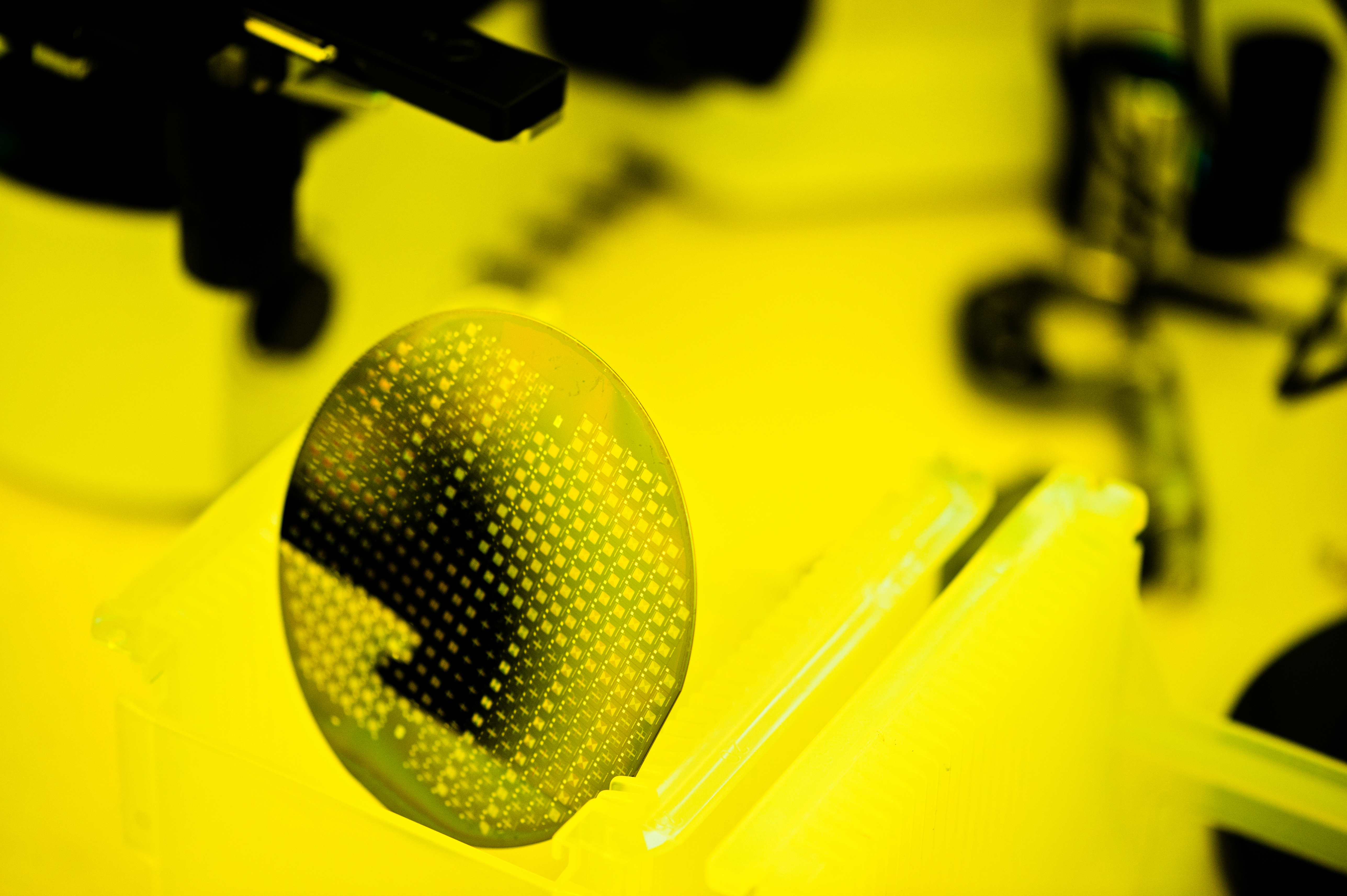
Cleaning Matters in the 3D Era
While some people believe Moore’s Law is running out of steam, the chip industry continues to scale semiconductor devices into the third dimension, increasing transistor density with every new chip generation. The semiconductor transistor continues to evolve, moving from planar to FinFET to gate-all-around (GAA) structures. The memory side of the business has been building 3D NAND structures since 2013, and DRAM is moving to 3D due to the process complexity of shrinking trench capacitors into the 10 nm range.
The smaller dimensions have made cleaning processes a front-line challenge for semiconductor manufacturing. Removal of contamination is critical for high yields and reliability, while increasingly fragile, high-aspect-ratio structures require tailored cleaning processes to remove contamination as well as to prevent these structures from collapsing, thus impacting yields.
Market Context and Technology Convergence
The demand for memory is increasing. As a result, the transistor continues to scale, and memory companies are looking for methods to meet the escalating demand. Introduced in 2013 at 24 layers, 3D NAND is now in production at 232 layers. 512-layer 3D NAND is in R&D, and 1032 layers are expected to start production around 2027, tripling the amount of memory on a chip in just a few years.
Deep-capacitor trench architectures in DRAM have continued to evolve to improve storage and latency. DRAM is moving to 3D architecture in 2025 and beyond, which increases the challenges for wafer cleaning technology. Residues, particle contamination, and pattern collapse are common across all semiconductor wafer technologies. The deep trench features of memory architecture demand sophisticated processes to remove contamination while maintaining the structural integrity of the transistor cell.
Deep Trench Cleaning for 3D NAND and 3D DRAM
The key challenges for deep trench cleaning of 3D NAND and 3D DRAM include high-aspect-ratio trenches or cylinders of >50:1. The etching of these features leaves, deep within these vertical stacks, polymer residues that need to be removed. The pillars or cylinders can lean or collapse during the drying process, thus making the cell unusable so that good transistors cannot result.
ACM Research (ACMR) addresses these cleaning challenges using several advanced cleaning innovations:
- The Ultra C TEBO™ tool uses Smart Megasonix™ to control the cavitation, enabling thinning of the boundary layer. This allows cleaning chemistry to reach deep into narrow features, removing polymers from the dry etch without causing the lines to collapse.
- The SCCO₂ drying system ensures collapse-free drying after wet clean steps — particularly effective for 3D NAND’s stacked cell arrays and for sub-10 nm features expected in 3D DRAM.
The proven results show the removal of deep trench contaminants, enhanced yield by preventing pattern collapse, and support NAND and DRAM structures with chemistries designed specifically for the cleaning process step.
Unified Cleaning Platform for Memory
ACMR has developed a modular hybrid system wherein single wafer and batch processes can be combined on a single equipment platform. The TEBO™, Smart Megasonix™, SCCO₂, SPM and hot phosphoric bath technologies can be used stand-alone or as a combination of process chambers to meet the needs of cleaning advanced memory devices. Each single-wafer process step provides for optimum cleaning and etching performance across the wafer. The modular system allows for a sequential cleaning/etching process, followed by the drying process, on a single platform. The platform has programmable recipes that enable switching between different applications in the process fab.
Implications for Device Manufacturers
The integrated cleaning platform enables higher yields and a shorter ramp time for 3D memory technologies, as the number of layers increases from 200 to beyond 1,000, and cell dimensions shrink. The modularity of the ACMR high-aspect-ratio cleaning platform allows memory manufacturers to future-proof their fabs as new layers are added or different architectures are introduced. The platform’s process capabilities enable cleaner interfaces, which will facilitate more reliable advanced packaging and 3D IC device stacking.
Cleaning is a critical technology for the 3D structures in the memory process. Whether thousand-layer NAND, 3D DRAM capacitors or nanosheet transistors, precise cleaning is foundational to the success of semiconductor technology. ACMR’s platform, combining Smart Megasonix™ and SCCO₂ drying, offers the non-destructive, residue-free performance that you need to build the 3D structures of today — and tomorrow.