
As the feature sizes and critical dimensions of logic, memory and analog semiconductor devices shrink with advanced technology nodes, the sensitivity to submicron contaminants has increased significantly. Consequently, the use of wet cleaning technology to remove particulates and contaminants is critical to the success of semiconductor manufacturers.
Single-wafer and batch cleaning technologies are both used extensively across the manufacturing spectrum. Each offers different benefits from a cost and particulate-removal perspective, depending on the technology node and specified process sequence. In this blog, we explain the differences between batch and single-wafer cleaning technology and what customers should consider when choosing between the two for their cleaning requirements.
Market Context and Technology Convergence: Memory Devices and Advanced Packaging
The shrinking of technology nodes and the introduction of new 3D transistors and high-aspect-ratio features are creating significant challenges for semiconductor manufacturers. New transistor technologies, such as gate-all-around (GAA) and vertically stacked complementary field effect transistors (CFET), require advanced cleaning technologies to penetrate spaces that are mere angstroms wide.
At the same time, 3D-NAND is rapidly adding layers and is expected to have 1,000 layers by 2027, with aspect ratios approaching 100 to 1. Soon, DRAM aspect ratios will also approach 100:1. These features require the removal of not only particulate contamination but also hidden contaminants, such as residual metals and chemicals that can impact the performance of the semiconductor chip.
The rapid growth of 3D packaging also adds further challenges for wet cleaning. These chip dimensions require sophisticated cleaning techniques to remove residues and create clean surfaces at the bottom of these deep structures. Scarce water sources and a focus on sustainability require creative solutions to reduce the use of clean water in the rinsing process.
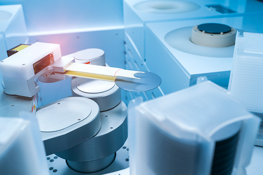
The Differences Between Batch and Single-Wafer Wet Processing
The table compares the features of the two cleaning technologies and provides insight into tool selection.
| Feature | Batch Tool | Single-Wafer Tool |
|---|---|---|
| Throughput | High | Lower |
| Uniformity | Lower | Higher |
| Contamination Control | Moderate | High (essential for advanced nodes) |
| Cost | Lower cost per wafer | Higher cost per wafer |
| Process Control | Batch-level control | Precise, wafer-level control |
| Typical Use | Mature nodes, standard cleaning | Advanced nodes (<45nm), high complexity |
Batch processing is the optimal choice for bulk strip and cleaning processes, such as photoresist removal or a wet etch, where all the material is removed. Batch processing is also considered the preferred technology for mature process nodes, where a lower cost of ownership is most important. Batch systems typically process 50 to 100 wafers at a time, making them more efficient for legacy devices.
The advantages of batch processing include high throughput, lower cost and reduced chemical consumption per wafer. However, some of the drawbacks include the risk of cross-contamination from backside particulates, reduced wafer-to-wafer control, and the potential for the entire batch of wafers to be scrapped if damage occurs during the process.
Single-wafer tools are ideal for advanced technology nodes where higher process control and precision are required (<45nm). Fragile or expensive substrates, such as silicon carbide (SiC), can benefit from single-wafer handling techniques as well.
Single-wafer tools provide superior process control, higher yield due to reduced defect density, less cross-contamination risk and faster processing. As a result, these tools also typically cost more than a batch system due to the added complexity and higher chemical usage. However, the process performance at advanced nodes typically outweighs these concerns.
Key Considerations
When choosing between a batch tool and a single-wafer cleaning system, there are several areas to consider.
One key factor is the uniformity of the clean or material strip as well as that of the contamination removal. On a wafer with flat or large geometries, a batch system may be sufficient. However, if there are small features that require optimized contamination removal, a single-wafer tool may be the better choice.
At advanced technology nodes, a single-wafer system gives you the ability to perform a backside clean and bevel removal needed to ensure optimal process performance for the ensuing steps.
Most importantly, the overall cost of ownership needs to be considered. It is important to take into account both the economics of chemical usage in a batch or single-wafer system and the wafer throughput of the overall process.
ACM’s Wet Processing Tool Portfolio and Competitive Advantage
We provide fully automated, enclosed batch and single-wafer cleaning solutions for analog, mixed-signal, 3D-NAND, advanced DRAM, advanced logic and advanced packaging applications. Our batch and single-wafer tools have achieved proven industry success using our proprietary megasonic Space Alternated Phase Shift (SAPS™) and Timely Energized Bubble Oscillation (TEBO) technologies for enhanced residue removal. They also achieve superior residue-free wafer drying using hot isopropyl alcohol (IPA) and supercritical carbon dioxide (scCO2).
We offer a hybrid batch/single-wafer solution on our Tahoe platform for maximum process flexibility. These cleaning systems offer superior process control and have proven success across the semiconductor industry, ensuring excellent within-wafer uniformity and defect control for leading-edge semiconductor device manufacturing.
Implications for Semiconductor Manufacturers
With years of proven process and service experience in wet cleaning technology, our industry-leading batch and single-wafer wet processing technologies are designed to address critical challenges for advanced device manufacturing nodes, as well as for wafer-level packaging (WLP) and panel-level packaging (PLP) applications.
Leveraging our world-class tool design, engineering teams and process technology experts, we can assist you in selecting the right equipment to meet your process specifications for wafer cleaning across all technology nodes.
Reach out to our team today to learn more at contact@acmr.com.