
It’s not news that artificial intelligence (AI) is driving larger and larger chip packages. For example, Nvidia’s Blackwell architecture is what is called a two-reticle package1, meaning that the chips each have an area of approximately 800mm2. Building chips and packages of this size poses myriad challenges – one of which is how many 800mm2 chips can fit on a 300mm wafer.
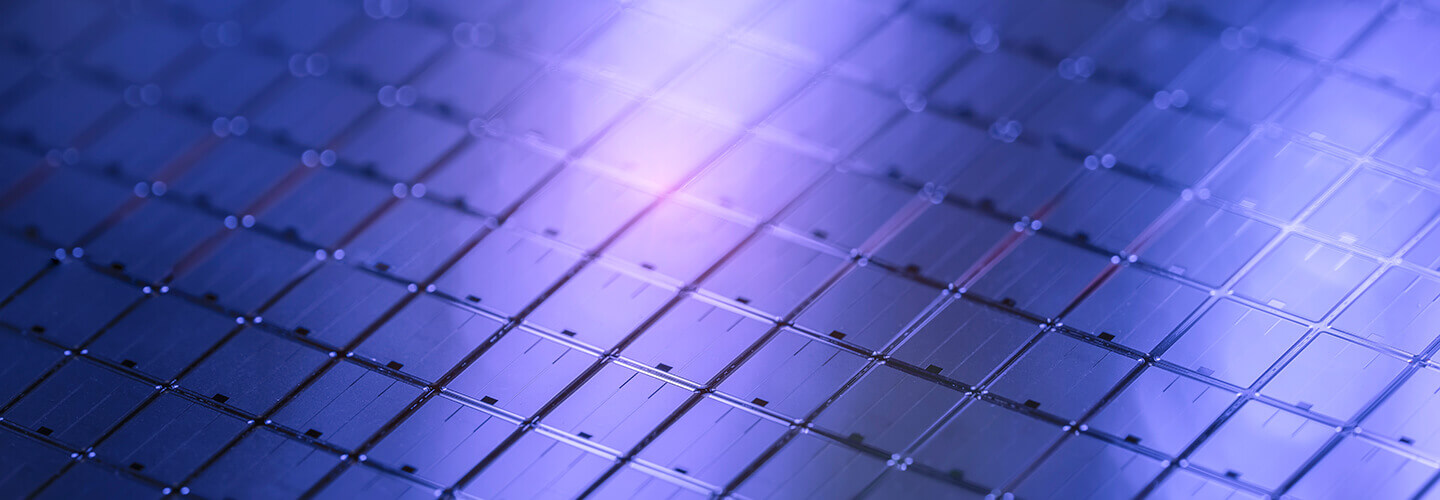
With a chip size of ~800mm2, you can fit approximately 64 chips on a round 300mm wafer. However, this does not consider yield. As the chip is square and the wafer is round, a significant amount of silicon goes to waste in processing the chip.
When it comes to wafer-level packaging (WLP) or fan-out wafer-level packaging (FOWLP), you run into the same problem. You are limited by the area of the silicon wafer, thus causing throughput and yield problems during the packaging process. TSMC’s chip-on-wafer-on-substrate (CoWoS), the current method of packaging Nvidia’s advanced chips, has capacity and yield constraints, according to TSMC earnings calls.
FOPLP (Fan-Out Panel-Level Packaging) Enables System Package Creation
Given these challenges, fan-out panel-level packaging (FOPLP) has attracted interest and attention from the semiconductor industry. To help solve the packaging side of the supply chain constraint, packaging manufacturers have proposed using square substrates, typically made of glass, to introduce a new method of packaging the wafers on a panel that increases the number of chips you can process at once.
The industry, for now, has settled on panel sizes of 515mm x 510mm, which has 3x the area of a 300mm silicon wafer; and 600mm x 600mm, which has 5x the area of a 300 mm wafer2 (Figure 1). Intel, Samsung, and some outsourced assembly and test (OSAT) companies are also moving toward panel-level packaging (PLP). This is due mainly to the growth of AI chip packages, which, as they continue to grow increasingly larger, are becoming systems, rather than individual packages placed upon a printed circuit board (PCB).
Figure 1. A 300mm wafer compared to 515mm x 510mm and 600mm x 600mm panels. (Source: ACM Research)
Tackling panel-level packaging bevel etch and clean
The transition to Panel-Level Packaging (PLP) will create new processing challenges that will require a new set of tools. Cleanliness and thickness at the panel edges are critical for yields and processing. Contamination or a raised edge bevel can create issues for lithography, deposition, and bonding and can potentially generate stress, which can cause warpage across the panel.
The ability to clean effectively across an entire panel to remove flux residues and particles will also be a critical part of the move to PLP. This requires proper handling of the panel as well as ensuring it is dry before the next process steps take place. The deposition and removal of metals for redistribution layers (RDLs), pillars, and bumps will play an important role in the creation of both the RDLs and the chiplets.
As a company that enables advanced WLP with our cleaning and deposition equipment, ACM Research recently introduced three new tools to address the industry’s move to PLP. Given our expertise in both cleaning and electrochemical plating, these tools fit seamlessly into our portfolio and will help our customers move from WLP to PLP technology.
- Ultra C bev-p panel bevel etching tool – Designed specifically for panel substrates, Ultra C bev-p offers compatibility with organic, glass, and bonding panels. The system enables advanced panel handling with a single robot, efficient copper removal using diluted sulfuric acid and peroxide (DSP), and high throughput of 40 panels per hour.
- Ultra C vac-p flux cleaning tool – This tool addresses critical steps in the advanced packaging process on organic and glass panels, particularly removal of flux residue before underfilling, which is essential for eliminating voids. Its vacuum technology ensures cleaning liquid reaches all gaps, even in large panel substrates where traditional methods fall short.
- Ultra ECP ap-p tool – Our panel-focused electrochemical plating (ECP) tool supports 515mm x 510mm glass and organic panels, with an option to expand to 600mm x 600mm. Its horizontal plating approach achieves superior uniformity and precision across the entire panel, and its advanced automation features enhance manufacturing efficiency and quality control.
Our new tools are designed to work together to meet emerging PLP requirements, including multiple-reticle PLP, to help the industry quickly move forward in the transition from WLP.
Panel Level Packaging FAQ
References
1Shilov, A., “NVIDIA’s Next-Gen Blackwell GPUs Rumored To Use Multi-chiplet Design,” Tom’s Hardware, September 2023.
2“TSMC Reportedly Forms a Team on FOPLP Development, with Mini Line on the Road,” Global SMT & Packaging, July 2024.