
Throughout this blog series, we’re examining vital wafer cleaning processes and how we are addressing them through our solutions. In this post, we’ll look at bevel etch: what it is, associated challenges, and how our approach offers notable advantages for tackling those challenges compared to traditional dry bevel etch.
The bevel etch process is used to remove any type of film on the edge of the wafer, whether the film material is dielectric, metal, organics, silicon nitride and silicon oxide. During bevel etch, the wafer is held by a top and bottom plate, so that the wafer edge is the only exposed part of the wafer. The simplified diagram in Figure 1 below illustrates that the wafer bevel edge is not totally flat but is actually slightly rounded above and below the apex. Accumulation of particles and peeling at the wafer edge create contamination that can lead to yield loss. Bevel etch and clean processes prevent these problems from occurring.
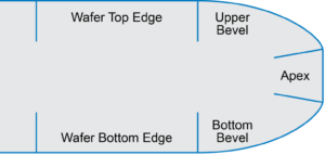
Figure 1. The transition from a planar surface to the wafer bevel and apex regions creates a high-stress area susceptible to film delamination, or peeling.
Market drivers
Process integration complexity and defects are increasing in key markets, including manufacturing of 3D NAND flash devices, as well as DRAMs and advanced logic ICs. This is due, in part, to larger stack deposits and increased variations in thickness between the wafer center and the wafer edge. These advanced devices require high accuracy and efficiency in wafer alignment, as well as highly precise removal of any particulates and other potentially damaging material residue during bevel etch and clean.
The 3D NAND flash memory market is expected to experience significant growth. According to Allied Market Research, the global 3D NAND flash market is projected to reach US $78.2 billion by 2030, representing a CAGR of 20.3% between 2021 and 2030. Key factors behind this growth include improved performance and lower latency of 3D NAND devices, as well as heightened demand for data centers – a primary consumer of these memories.
Challenges and ACM’s approach
While much of the bevel is created during film deposition, the films deposited are not uniform at the edge of the wafer. Combined with the fact that the wafer itself is slightly elliptical in shape, this presents challenges for the bevel etch process. Historically, manufacturers have used a dry bevel etch process to address edge film and contamination removal. However, this technique can create arcing and risks damage to the silicon. Moreover, if the wafer is not centered, precise etch and clean of the bevel edge are difficult to achieve, heightening the likelihood that particulates will be left behind, compromising device manufacturing yield and performance.
Bevel etch is performed in the front end before copper metallization and in the back end after copper metallization. ACM attains superior results with our single-wafer Bevel Etch system, which combines bevel and backside cleaning. The system centers and aligns the wafer automatically on the vacuum chuck prior to cleaning – this is a significant competitive advantage for us, as other systems typically require manual centering. Once centered our system performs bevel clean on the wafer, sensors in the chamber makes sure the wafer remains centered. The next step requires the wafer to be flipped and cleaning of the backside. As the wafer spins, ACM performs non-contact cleaning, providing superior cleaning with wet bevel etch.
Our wet Bevel Etch product leverages our wet processing expertise to deliver significant performance benefits compared to dry approaches, and consumes significantly reduced amounts of chemicals. With our proprietary technology, the system’s more accurate and efficient wafer center alignment enables it to deliver precise bevel etch that will enhance product yields and wafer throughput. Our wet etch approach avoids the damage risk from the dry process, while offering variable wafer bevel etch/cut accuracy of 1-7mm, good uniformity of +/-0.1mm, controllable etch selectivity and low chemical consumption, for a lower total cost of ownership.
Promising results
The ACM Bevel Etch product has been installed at leading customer sites, and the data we’re seeing from this installation illustrates the benefits of the technology. Bevel SC1 and DHF etch 1mm testing on wafers using titanium nitride and silicon oxide films, respectively. With narrow cut widths, the process yields excellent uniformity – 2.22% and 3.16% for TiN and ThOX.
We look forward to continued strong results as sales of our Bevel Etch system increase in concert with rising advance memory and logic manufacturing.