
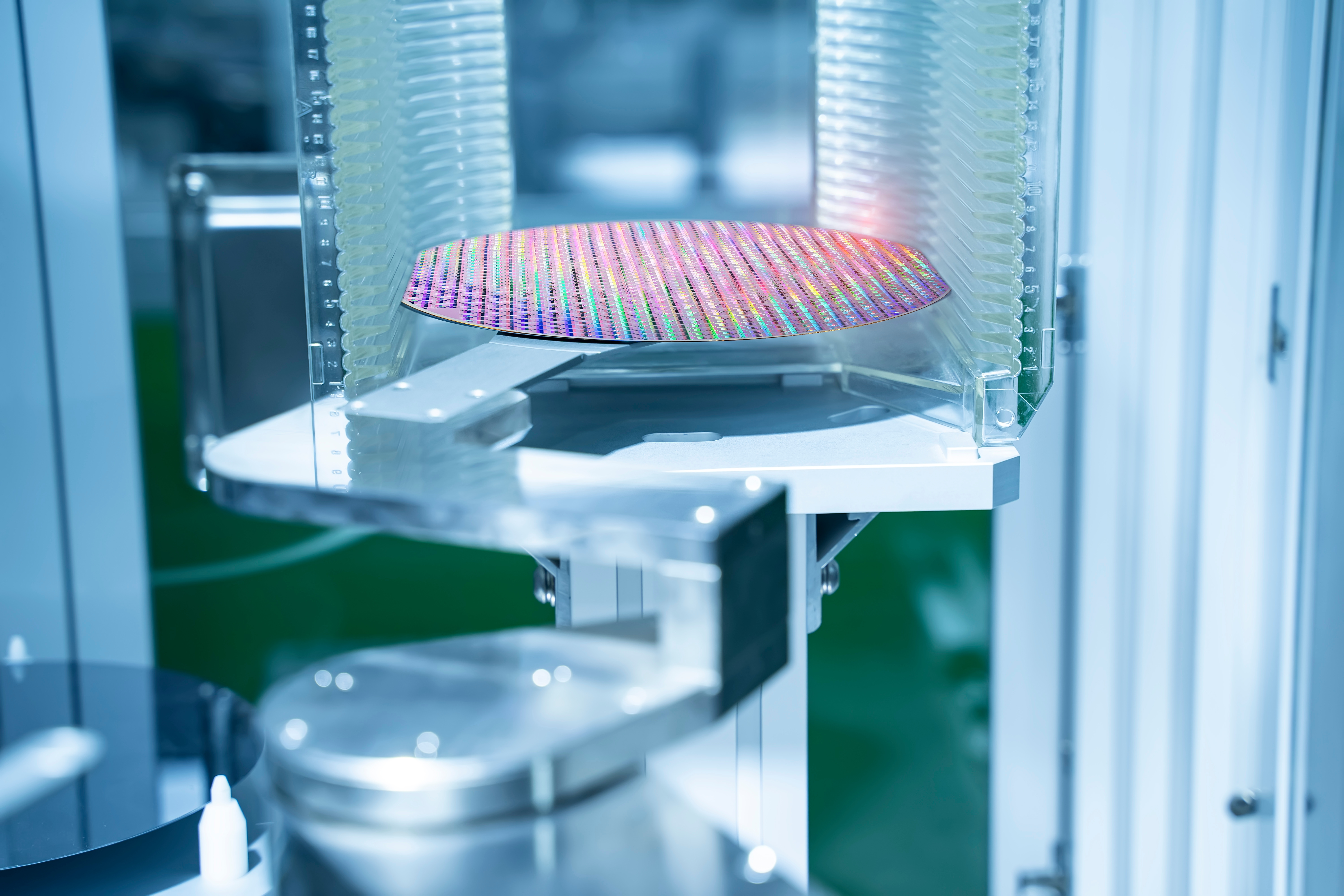
Plasma-enhanced chemical vapor deposition (PECVD) has been a critical part of the semiconductor manufacturing process since the 1980s. With chipsets designed for AI applications transitioning from wire bonding to 2.5 and 3D packaging, PECVD processes have rapidly gained importance within the heterogeneous manufacturing process. PECVD enables the deposition of high-quality dielectric films for 3D packaging integration in applications such as through-silicon via (TSV) passivation, hybrid bonding, and insulation of metal layers.
Deposition Challenges and Uniformity Requirements for AI Chips
The rapid growth of AI has been facilitated by advanced packaging. As a result, advanced packaging is growing rapidly to meet the demand for AI chipsets, creating manufacturing bottlenecks in the packaging process. Advanced packaging needs excellent uniformity and dielectric step coverage for the TSV liners used in 2.5 and 3D packaging processes.
TSVs are used to stack the chips together to form 3D structures, and hybrid bonding requires uniform dielectric layers to ensure good bonding across the die or wafers. PECVD is the ideal tool for each of these process steps in the advanced processing manufacturing flow.
As AI chipsets growth escalates, high-throughput tools are needed to meet the high demand. The common deposition challenges for packaging are achieving both good deposition uniformity across the wafer and good step coverage across the entire wafer or packaging substrate. Low levels of contamination are a must to realize high yields in the final product. Additionally, film quality and precision – across the wafer, across the lot of wafers, and from lot to lot – are crucial for delivering consistent electrical performance in the thousands of AI chipsets delivered to the customer. ACM Research developed the Ultra PmaxTM PECVD tool to address the needs of the advanced packaging market. Here are some of the key benefits.
Excellent Film Coverage and Uniformity
Our Ultra PmaxTM delivers best and uniform film coverage across the wafer or substrate area and from lot to lot. The Ultra Pmax achieves its excellent uniformity by using a special focus ring that controls and balances the radial/azimuthal gas flow across the wafers. A dedicated RF power supply and impedance match for each wafer station, along with focused gas flow and ability to rotate the substrate in between depositions without stopping the plasma, are key components for achieving excellent film uniformity.
To attain industry-leading TSV step coverage as well, we implement automated shower tilting and heater-leveling optimization, which enables gap tuning. By combining all of the features mentioned above, the Ultra Pmax achieves best-in-class uniformity and industry-leading 40% step coverage for vias with a 5:1 aspect ratio.
Stress Management for PECVD
Stress management of deposited films is critical to advanced packaging. High stress can lead to cracking and delamination, rendering the chipset unusable, or worse, having it fail after it has been placed inside a server. Managing film stress helps to maintain the structural integrity of both the chip and the final package. Our tool manages stress with a dedicated RF power supply and impedance match for each wafer process station. A rotating heater and control of the deposition pressures allow the Ultra PmaxTM to optimize stress in thin or thick film deposition.
Optimal Flexibility and Wafer Throughput
Designed to optimize wafer or substrate throughput, the highly flexible Ultra Pmax can be configured for R&D and subsequently reconfigured for high-volume manufacturing, as the process module design allows three wafers to be processed simultaneously. The Ultra Pmax can be configured with up to five process modules, which enables as many as 15 wafers to be processed at once. This gives customers ultimate flexibility when it comes to wafer-throughput configuration.
Achieving High-Yield and High-Performance Devices
Our Ultra PmaxTM PECVD tool provides optimized dielectric films for TSV and hybrid bonding applications for 300mm wafers or substrates. The films provide excellent barrier layers for the copper plating process and provide advanced packaging manufacturers with a state-of-the-art tool for processing.
As AI chipsets drive the demand for increasingly sophisticated packaging solutions, PECVD has emerged as a foundational technology for achieving the precision, uniformity, and reliability required in 2.5D and 3D integration. Innovations like ACM Research’s Ultra Pmax platform, with its advanced control over film stress, step coverage, and deposition uniformity, ensure that PECVD continues to be instrumental in overcoming the complex challenges of heterogeneous integration and delivering high-yield, high-performance AI devices.