
Silicon carbide (SiC) and gallium nitride (GaN) are becoming mainstream within the semiconductor industry due to material properties that make them ideal for multiple applications. These properties—ranging from high thermal conductivity and mechanical strength to optical refractive index control—have made SiC and GaN suitable candidates for multiple end products.
Some key applications include power and battery management in electric vehicles; power switching and management in renewables and the electrical grid; power management and energy saving for data centers and electronic devices; and high-frequency characteristics for next-generation communications, including multifunctional optical architectures. SiC and GaN semiconductors can manage higher voltages in a smaller form factor, switch power more quickly, and run significantly cooler, which saves energy costs and improves system performance, as producing less heat enables systems to run at lower temperatures.
Tackling Material Challenges of SiC and GaN
Their remarkable material properties also make processing GaN and SiC wafers in a semiconductor manufacturing facility more challenging. The materials are extremely hard and brittle, with higher thermal sensitivity than silicon, and the wafers are often thinner. These properties can lead to edge chipping, wafer bowing and stress during processing. This requires both sophisticated wafer-handling equipment to accommodate thinner wafers and unique process parameters to prevent wafer-surface chipping and particles, which lead to defects and, in turn, chip failure.
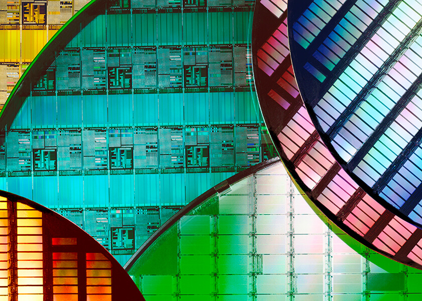
Because SiC and GaN semiconductors are mature technologies, multiple wafer sizes are being used in the manufacturing process. There are 4-, 6-, and 8-inch wide-bandgap semiconductor factories in volume production, as well as 12-inch, or 300mm, facilities coming online as the technology to produce 300mm wafers emerges for both SiC and GaN. To meet the industry demand for high-quality wide-bandgap semiconductor processes, we developed sophisticated wafer-handling technology and cleaning-process technologies that can be used across all wafer sizes. Our equipment can delicately handle brittle SiC and GaN wafers, as well as very thin wafers that may have stress-induced bowing.
The Vital Role of Cleaning Technology
Cleaning technology is a critical component of the transition from silicon to SiC and GaN chips in the power semiconductor industry. We have been working with our customers on SiC and GaN processing for more than five years and developed a wide portfolio of cleaning processes for SiC and GaN chips. We created cleaning and wafer-handling systems specifically designed to accommodate SiC and GaN materials’ complex handling requirements. Our cleaning processes deliver wafers with low defect levels, thus ensuring high-yielding chips at the end of your process flow.
At ACM Research, we adapted our deep understanding of silicon surface chemistry, defect mechanisms and single-wafer process control to the unique material properties of SiC and GaN wide-bandgap semiconductors. This broad selection of cleaning processes and handling techniques developed for GaN and SiC enables precise removal of hard-to-clean residues and particles while preserving the materials’ delicate surfaces. This surface cleanliness is critical in GaN and SiC process flow, as any surface defects can cause imperfections in the epitaxy layer, potentially leading to lower yields.
SiC and GaN Device Scaling
Our dedication to developing superior cleaning technologies for wide-bandgap markets allows our customers to process defect-free surfaces, helping you to achieve higher yields and reliability as you scale SiC and GaN semiconductor manufacturing. Reach out to our team today at contact@acmr.com.