


Advances in automotive, high-performance computing (HPC), artificial intelligence (AI) and medical technology are heightening demand for heterogeneous integration. As a result, the semiconductor packaging industry is being driven to develop large multi-reticle packages.
To process the massive amounts of data being generated, chip and package sizes have grown significantly. Chip sizes are using the full reticle window of 858 mm2, and manufacturers are integrating chips the size of 5.5 reticles into advanced packages. For example, TSMC’s roadmap is anticipated to surpass a combined 14 reticles in 2029.
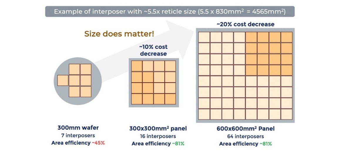
With this shift, large-reticle packages are creating both throughput and yield challenges for the industry. The massive NVIDIA H100 is a 1600mm2 package with 80 billion transistors—far too large for round substrates, which can produce 35 packages at most. This limits packaging throughput and can cause yield issues, as the die closest to the edge may be affected by damage and particulates.
Transitioning from a round substrate to a square panel enables more packages per substrate area and can significantly improve throughput, yield and cost reduction. Yole Group projects that the market size for panel-level packaging (PLP) will grow rapidly at a 40% compound annual growth rate (CAGR) through 2030, as shown in Figure 1.
Semiconductor Packaging Industry Status
Multiple semiconductor manufacturing companies and outsourced semiconductor assembly and test providers (OSATs) are increasingly pursuing PLP manufacturing. Samsung, ASE/SPIL, Amkor and Power Tech have fan-out wafer-level packaging (FOWLP) lines in production, while TSMC and Intel have packaging lines in development.
One reason companies are making the shift to PLP is that the smaller area of the round substrates impacts supply. With a larger area, more packages can be processed simultaneously. Yields also improve, as die at the edge of the panel may be less impacted by contamination. Manufacturers are learning how to handle quartz panels, which can flex and have a different coefficient of thermal expansion (CTE) than silicon chips, which can cause warpage.
As PLP process technology continues to mature, several processing challenges have slowed its implementation. Issues such as adhesion of the package substrates to the panel, along with the uniformity of copper deposition across the panel and in the vias, remain a work in progress. The lack of panel standardization is also a major concern, as there is a large area difference between 600x600mm panels and 310x310mm panels. Addressing these challenges requires equipment companies to design tools and processes that can support all three substrate sizes.
ACM Research’s Advanced Packaging Solutions
ACM Research offers multiple process solutions for advanced packaging, for round substrates and three panel sizes. These processes can be utilized in OSATs’ development labs for panel cleaning, bevel strip and clean, copper plating and flux removal.
We developed specialized handling of large substrates for both glass and organic substrates from 310x310mm to 600x600mm. The Ultra ECP ap-p plating system has a unique multi anode, which is a key enabler for highly uniform copper deposition and adhesion. The careful chamber design and process development provide industry-leading plating uniformity.
The Ultra C vac-p flux cleaning tool provides superior vacuum-based cleaning technology for the removal of contaminants in hard-to-reach spaces, especially in the bumping process. The Ultra C bev-p double-sided bevel etching tool can perform both bevel etching and copper removal for PLP.
Our PLP tool portfolio can handle 310x310mm, 510x515mm and 600x600mm panels with thicknesses ranging from 0.5mm to 3mm and warpages of ≤10mm. The tools are proven to have panel breakage of <1/50,000, demonstrating the robustness of the panel-handling system.
The tools also come with two or three load ports, depending upon the given process technology, and all our tools have a mean time between failures (MTBF) of >500 hours. The chambers are designed for processing the panels in a horizontal position and provide the optimum process conditions for film deposition uniformity, with uniformities of <5% (max-min/2Ave.) for both across the wafer and within the die. The Ultra C bev-p tool performs a superior bevel clean with bevel control accuracy of ±0.2mm.
Leveraging our long-standing history of deposition and cleaning experience, ACM Research has enabled industry-leading process technology for PLP.
Real-World Applications
The Ultra ECP ap-p supports multiple plating applications, including pillar, bump and redistribution layer (RDL). The panel plating equipment can also be utilized for micron and submicron high-density PLP. The unique multi-anode system and the horizontal panel positioning provide excellent uniformity and have also demonstrated exceptional adhesion to glass panels.
The Ultra C bev-p tool’s innovative design ensures a precise bevel-removal process that remains confined to the bevel region, even on warped panels. This advancement is vital for maintaining the integrity of the etching process and achieving the high performance and reliability required by advanced semiconductor technologies. This process is crucial for preventing electrical shorts, minimizing contamination risks, maintaining the integrity of subsequent processing steps and ensuring the long-term reliability of devices.
The Ultra C vac-p addresses critical steps in the advanced packaging process, particularly the removal of flux residue before underfilling, which is essential for eliminating voids, offering strong benefits for fan-out panel-level packaging (FOPLP), chiplets and 2.5D/3D structures. Traditional cleaning methods often fail with small bump pitches (<40 µm) and large chip sizes due to surface tension and limited liquid penetration. The vacuum technology in the Ultra C vac-p flux ensures the cleaning liquid thoroughly reaches all gaps, even in large panel substrates where traditional methods fall short. Combined with our proprietary isopropyl alcohol (IPA) drying technology, this comprehensive cleaning process prevents residues that could impair device performance.
ACM Research brings to the industry decades of experience in wafer cleaning, electrochemical plating and wafer-level packaging. As the transition from wafer to panel evolves, we continue to innovate and develop cutting-edge equipment for processing wafers, meeting the demand for heterogeneous integration.