

Part 1 of this series examined cleaning challenges associated with panel-level packaging (PLP) and manufacturing. This installment goes into some of the key industry and market drivers spurring PLP demand.
Multi-reticle packages are growing at a rapid rate. Figure 1 shows TSMC’s advanced packaging roadmap growing from 5.5 reticles today to 14 reticles in 2029 (between 2x and 3x growth in package sizes).
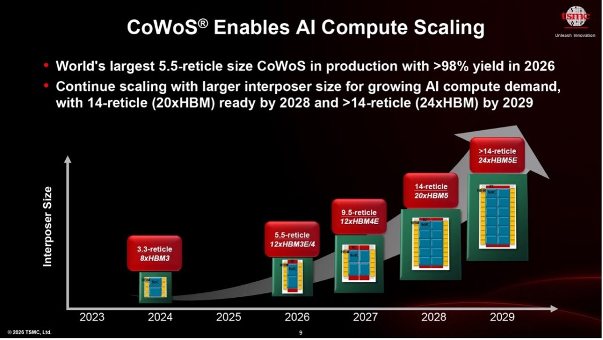
As the figure indicates, it’s expected that by 2029, 40 chips will be integrated into 14-reticle packages,10 large compute die and 20 high-bandwidth memory (HBM) stacks. Each stack will have 16 HBM DRAMs, giving each package an immense amount of computing power.
This growth in large packages is being driven by the insatiable demand for high-performance computing (HPC) to support the growth of artificial intelligence (AI). In turn, AI, medical and automotive applications are driving the industry transition from a system on a printed circuit board (PCB) to a system in a package.
The strong demand for multi-reticle packages is creating shortages for HPC customers. Packaging companies are struggling to keep up with demand due to the current packaging technology, as the industry currently uses wafer-level packaging (WLP), which means a 300mm round substrate is used to process large packages. Area constraints limit the number of these large packages that can be processed on round substrates. Yields can also suffer from packages that are too close to the edge of the wafer.
On the other hand, PLP uses square panels to support the packaging substrates. This creates a larger surface area that can fit more packages on each panel. Panel sizes are currently 310x310mm to 600x600mm. Using larger substrates and connecting chips more effectively creates greater bandwidth and reduces system latency—in turn, improving overall system performance.
Packaging Industry Pain Points
The demand for AI and HPC packages for data centers is outpacing how fast they can be manufactured. The source of the constrained supply is thought to be the packaging process. Currently, round substrates can fit about 30 to 35 packaged die; using panels would increase productivity considerably. While a few 310x310mm panel packaging facilities are emerging, there are some challenges facing the industry.
First, there is a lack of PLP process equipment and technology. While the basic process chemistries can work, the processes need to be optimized for panel substrates. For example, modifications need to be made to the copper process to ensure good adhesion and uniformity across the panel.
Tools need to be configured to handle square substrates, and modifications need to be made for handling substrates that may have warpage. The lack of a standard panel size creates prioritization challenges for equipment makers when different customers may be using different panel sizes.
Why Move to Panel-Level Packaging
Moving to PLP increases flexibility for packaging manufacturers. It better supports the integration of the different chiplets onto a single package. This leads to improved system performance, as the resulting packages can be thinner and smaller, which makes them more suitable for HPC, automotive, medical and other applications where size and power performance are critical.
Panel-level packaging reduces chip handling and can lower the potential for contamination and improve yields due to reduced process impact on the die at the edge of the round substrate. The larger panel area also means more packages per substrate, which can significantly improve throughput.
ACM Bolsters Transition from Wafer to Panel
ACM Research has been delivering packaging solutions for more than 10 years, helping to enable a smooth transition from wafer to panel. Within our PLP tool portfolio, we offer an electrochemical plating (ECP) and planarization tool, a unique flux cleaning tool that ensures total flux removal, and a bevel edge solution with cleaning and high bevel control accuracy.
Providing industry-leading surface cleaning and particle removal, our portfolio of tools can handle 310x310mm, 510x515mm and 600x600mm panels. We have developed processes for all the different panel sizes, focusing on delivering industry-leading plating adhesion and non-uniformity of < 5% using our multi-anode technology, edge bevel control of ±0.2mm around the panel, and industry-leading vacuum technology to ensure optimum yields. The process equipment features two or more load ports and process chambers that can be optimized for either technology development or the addition of chambers to maximize fab production.
The demand for large packaging solutions is driving PLP forward at a rapid rate. By 2029, packages with over 40 chips will need to be delivered in high volume to meet the industry’s needs. Our solutions, ready today for all panel sizes, will help the industry meet this demand in the future.