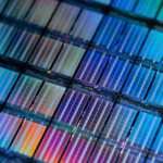
July 15, 2025 ~ Plasma-enhanced chemical vapor deposition (PECVD) is one of the fundamental building blocks for manufacturing ICs. From building the transistor to metallization, the PECVD process has applications critical for microelectronics manufacturing. PECVD allows to create a desired reactive gas plasma to deposit a thin film on the wafer. Typically, PECVD tools are used in manufacturing most […] Read More

Blogs and Articles
June 30, 2025 ~ Cleaning Matters in the 3D Era While some people believe Moore’s Law is running out of steam, the chip industry continues to scale semiconductor devices into the third dimension, increasing transistor density with every new chip generation. The semiconductor transistor continues to evolve, moving from planar to FinFET to gate-all-around (GAA) structures. The memory side […] Read More
June 23, 2025 ~ International Women in Engineering Day is about recognizing and highlighting the achievements of women in engineering and encouraging more women to enter the field. Despite progress, women made up just 13.7% of the global engineering workforce in 2023, with men representing 86.3%1. Engineering offers an exciting and varied career, full of new challenges every day, […] Read More
May 27, 2025 ~ High-performance computing has been reshaping the semiconductor industry for more than a decade. The explosive growth of computing power needed for artificial intelligence (AI) has been driving hyperscale data centers, which in turn, have been driving the need for high-performance semiconductor systems. The concept of packaging logic chiplets with high bandwidth memory (HBM) into multi-reticle […] Read More
March 31, 2025 ~ This year, we’re again incredibly proud to sponsor FIRST® Robotics Team 4488 SHOCKWAVE from Glencoe High School, a local school near our Hillsboro, Oregon facility. FIRST (For Inspiration and Recognition of Science and Technology), a global nonprofit founded in 1989, is dedicated to inspiring young people’s passion for STEM (Science, Technology, Engineering, and Math) while […] Read More
March 12, 2025 ~ Multi-reticle packages – optical devices with multiple reticle patterns that are user-switchable as needed – are becoming increasingly common as hyper-scale computing and other applications such as artificial intelligence (AI) adopt 2.5D to 3.5D device packaging. The advanced packaging industry, in turn, is implementing larger, panel-level packaging (PLP) to improve yield and increase throughput for […] Read More

January 13, 2025 ~ The 3D packaging sector has been growing rapidly, driven by the expansion of chiplet packaging across the ecosystem. Chip and package sizes have also grown rapidly as 2 x 800mm2 chips are being placed in a single package along with high-bandwidth memory (HBM). Demand for these large chiplets has generated supply constraints due to how […] Read More

November 26, 2024 ~ It’s not news that artificial intelligence (AI) is driving larger and larger chip packages. For example, Nvidia’s Blackwell architecture is what is called a two-reticle package1, meaning that the chips each have an area of approximately 800mm2. Building chips and packages of this size poses myriad challenges – one of which is how many 800mm2 […] Read More
October 15, 2024 ~ Throughout this blog series, we’ve taken you on a journey through the various steps involved in developing and optimizing through-silicon vias (TSVs), which have become vital to packaging of many types of devices that require smaller-footprint, higher-density package stacks. Part 1 discussed TSV formation and the benefits of our SAPS™ megasonics for TSV cleaning; Part […] Read More

August 29, 2024 ~ ACM Research provides an advanced solution for dealing with TSV Gaps using Plasma Enhanced Chemical Vapor Deposition (PECVD) Welcome to part three of our blog series on optimizing through-silicon vias (TSVs), vertical interconnect structures vital to heterogeneous integration of multiple components for 2.5D/3D packaging techniques. Part one provided an introduction to the TSV formation process […] Read More