

Wafer cleaning is one of the most critical steps in the semiconductor process flow, especially as dimensions continue to shrink to below the 1-nanometer (nm) node. Photoresist residue and particulates can reduce yields in large-die AI chips, impacting the performance of the final product or causing the chips to be scrapped.
The sulfuric acid hydrogen peroxide step, or sulfuric peroxide mixture (SPM), is essential for removing organic contaminants from post-etch substrates and ion-implanted films, as well as for platinum silicide residue removal. SPM processes traditionally have been performed in tanks or baths, which allows sulfuric acid to be reused multiple times by refreshing the chemistry with hydrogen peroxide.
However, in a bath or tank, undissolved photoresist can leave behind particulates, leading to defects in the process. Single-wafer systems can reduce particulates, but splatter and sulfur particles reforming from the mist in the chamber can leave chemical residue on the wafer, which can also impact yields for large-die chips. In addition, single-chamber systems can have lower process throughput due to the preventive maintenance required every two to three days to remove particles from the chamber.
Single-Wafer SPM Advantages
To address chemical surface contamination, ACM Research re-engineered the chamber and designed a patented cover and cleaning process for the spray nozzle. Our single-wafer SPM tool features a proprietary nozzle cover (Figure 1) that prevents acid mist splatter and reduces acid gas emissions by up to 90%.

This design minimizes particle buildup on the nozzle and chamber, resulting in improved cleanliness of the chuck, pin and nozzle cover. The nozzle cover, which delivers the SPM and also exhausts the vapors, is rinsed following processing of each wafer.
Customer cycle data shows reduced particle levels and chemical buildup, enabling:
- Extended preventive maintenance cycles, from every two to three days to every 30 days
- Reduced chamber cleaning time, from ~48 hours per month to less than two hours.
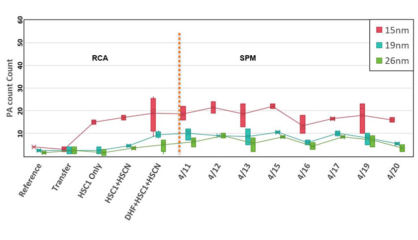
- Stable particle performance at 15nm over a 30-day operating period, providing matching or better results compared with traditional RCA cleaning processes (Figure 2).
By enabling SPM particle performance that matches or exceeds traditional RCA cleaning processes such as SC1 (Standard Clean 1), the system can improve overall process yield from approximately 70% to greater than 90%, supporting more efficient high-volume wafer processing. These improvements significantly increase system uptime and lower the overall cost of ownership.
Key Features of ACM’s Single-Wafer SPM Tool
ACM’s Single-Wafer Moderate/High-Temperature SPM tool has several unique features to enhance process performance:
- The multi-level heating method ensures that the highest mixed temperature exceeds 230°C and is steadily controlled at all temperatures needed for SPM processes.
- The tool is equipped with an inline chemical mixing system and a configurable process chamber that accommodates various SPM mix ratios. It can also be integrated seamlessly with ACM’s patented SAPS and TEBO Smart Megasonix technologies to enhance organic contaminant removal and improve wafer surface preparation.
- Its SPM nozzle design prevents high-temperature SPM from splashing onto chamber walls and components. It achieves better particle control, with an average particle adder count of fewer than 10 at 19nm.
- The nozzle cover, which both delivers the SPM and exhausts the vapors, is rinsed in its home position between every wafer.
- The chamber atmosphere is significantly enhanced through high exhaust over the processed area.
- Preventive maintenance time is reduced to less than two hours.
Applications in Semiconductor Manufacturing
Our Single-Wafer Moderate/High-Temperature SPM tool is suitable for a variety of front-end wet-etching and cleaning processes, including low- to medium-temperature sulfuric acid cleaning at 90°C, high-temperature sulfuric acid photoresist stripping at 170°C, and ultra-high-temperature sulfuric acid metal liftoff at 190°C.
The tool is designed for various wet-etching processes and both single- and double-sided cleaning. It is compatible with a wide range of chemicals and cleaning processes and supports wet etching and wafer cleaning for front-end processes at 28nm and smaller technology nodes. By effectively removing organic defects while minimizing film loss, it outperforms most post-cleaning and photoresist wet stripping processes. Supporting wafer sizes from 150mm to 300mm, the system features four load ports, a configurable setup of eight to 18 chambers, a multifunctional chemical distribution system and a self-cleaning chamber.
As noted earlier, the addition of our proprietary nozzle cover design and automatic in situ clean prevents acid splatter and vapor buildup during the SPM process – improving particle performance, reducing cleaning frequency and preventive maintenance downtime, and demonstrating a stable particle level on a 30-day preventive maintenance cycle.
Single-Wafer SPM Cleaning Capabilities for Advanced Semiconductor Manufacturing
A key industry player in single-wafer cleaning technology, ACM Research has positioned its innovatively designed Single-Wafer Moderate/High-Temperature SPM tool as a ready-to-deploy solution to meet evolving industry needs. The details of this tool and its capabilities were shared during a presentation at SPCC 2026, SEMI’s Surface Preparation and Cleaning Conference. Attendees responded positively to the session, which explained how the tool achieved better or matching SPM process particle performance when compared with traditional RCA cleaning.
This exemplifies our ability to develop solutions designed to meet current demands while future-proofing facilities as technology nodes advance. Our full tool portfolio covers cleaning, electroplating, stress-free polishing, vertical furnace processes, track, PECVD, and wafer- and panel-level packaging tools, enabling advanced and semi-critical semiconductor device manufacturing. We are committed to delivering customized, high-performance, cost-effective process solutions that semiconductor manufacturers can use in numerous manufacturing steps to improve productivity and yield.
Reach out to our team today to learn more at contact@acmr.com.