

Welcome to Part 3 of our blog series on optimizing through-silicon vias (TSVs), vertical interconnect structures vital to heterogeneous integration of multiple components for 2.5D/3D packaging techniques. Part 1 introduced the TSV formation process and post-via cleaning, and Part 2 delved into the role electroplating plays in TSV creation.
In this installment, we look at how to deal with gaps that can occur in TSVs during the manufacturing process. As AI, high-performance computing (HPC) and data center applications drive unprecedented demand for bandwidth, power efficiency and compute density, advanced packaging has become vital to system-level innovation. Technologies such as 2.5D integration, 3D stacking, chiplets and high-bandwidth memory (HBM) increasingly rely on TSVs to provide high-density vertical interconnects that enable heterogeneous integration and improved system performance. However, the TSV manufacturing process often leads to internal defects and poses processing challenges that can impact yield, reliability and overall package performance.
How do TSV gaps occur?
As traditional transistor scaling returns have diminished, TSVs emerged as a solution for extending system-level performance. Packaging more devices vertically, using TSVs to enable the electrical connections, allows more functionality to be integrated into the package. However, with increasing numbers of circuits packed together, the precise creation of these vias and the formation of electrical connections through them become more critical than ever.
Let’s start with a silicon wafer of about 300 microns in thickness; then, using lithography, create TSV holes in a pattern based on the device structure, followed by redistribution layer (RDL) lines to create the circuits. If the TSVs are 50 microns in diameter, this would result in a 5:1 aspect ratio (i.e., the ratio of the depth of the TSV cavity to its diameter). The higher the aspect ratio, the more difficult it is to create a uniform TSV.
This challenge is becoming even more significant as advanced packaging architectures continue to evolve. AI processors and HBM devices increasingly require thousands of TSVs per package, making uniform dielectric coverage and defect-free via formation critical to both electrical performance and manufacturing yield. Even small variations in film thickness or coverage can contribute to leakage, reliability concerns or downstream integration challenges. Moreover, to produce the copper fill that creates the interconnect, a uniform silicon dioxide (SiO2) barrier layer is required to provide good coverage, especially at the bottom walls of the via, and prohibit copper migration.
All of this takes place during the via fill deposition step – before chemical-mechanical polishing (CMP) and plating. As you deposit the dielectric SiO2 barrier layer from the top, the challenge when dealing with a high aspect ratio is making sure that the sidewall of the via receives even and sufficient coverage. It’s essential to realize at least 40% coverage at the bottom wall of the via to ensure uniform film coverage and TSV performance to achieve the best electrical results.
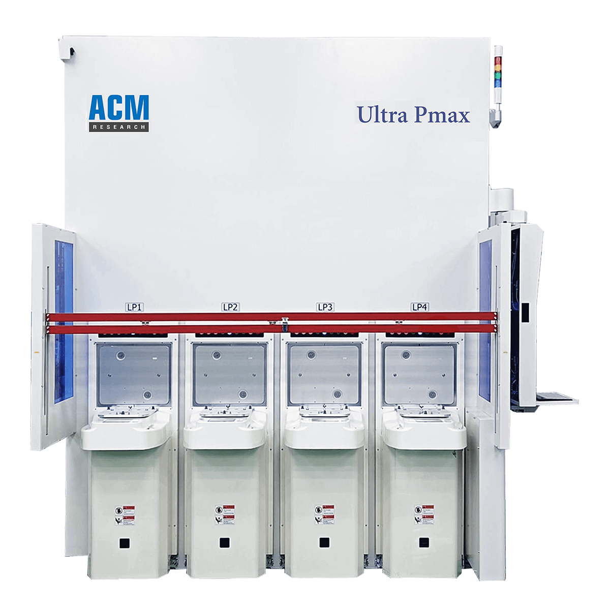
Conventional plasma-enhanced chemical vapor deposition (PECVD) technology is used for depositing a SiO2 barrier layer inside TSV via; however, the tools are challenged to deliver the necessary coverage, which can result in insufficient coverage at the via-bottom side wall. The Ultra PmaxTM PECVD advanced technology solution developed by ACM Research addresses the limitations of conventional PECVD technologies and provides excellent coverage at the high-aspect-ratio via bottom to enable optimal TSV gap fill.
Ultra Pmax™ PECVD – A better plasma option
Our Ultra Pmax™ PECVD technology, based on TEOS and O2 chemistries, is designed to address the demanding dielectric deposition requirements associated with advanced packaging applications, including TSV-based interconnect structures used in HBM, AI processors and heterogeneous integration platforms. The technology enables robust barrier layer formation in high-aspect-ratio TSV structures while maintaining excellent film quality and process uniformity. Its ability to accommodate low-temperature processing ensures better process control and evenness of layer thickness during the deposition process.
A pioneered and optimized PECVD TEOS-based SiO2 film from ACM Research can easily enable >50% coverage at the bottom, >65% at the center, and about 150% coverage on the top of the 5:1 aspect-ratio via. Any extra coverage on top of via can be easily reduced using CMP polish. ACM Research’s Ultra Pmax™ tool enables TSV application to deliver lower leakage current, higher dielectric breakdown and package reliability.
In general, our advanced Ultra Pmax™ PECVD technology is optimized for 300mm wafers to enable 3D IC integration for any type of device for both thin and thick film integrations. The tool is equipped with a proprietary designed chamber, gas distribution unit and chuck to deliver better film uniformity, reduced film stress and improved particle performance.
A unique aspect of the system is its proprietary (patent pending) process module design that integrates three stations and enables up to three wafers to be processed simultaneously, contributing to heightened throughput. Unlike competitive systems, each workstation has an independent, dedicated power supply and impedance match, ensuring within-wafer and wafer-to-wafer processing consistencies and film properties. The system can be converted from low-volume to high-volume manufacturing by integrating up to five process modules and two transfer chambers, depending upon the choice of the process module configuration.
Ultra Pmax benefits
High deposition rates
Our tool offers high deposition rates, significantly reducing processing times compared with traditional PECVD methods. This increased throughput translates to higher productivity and lower manufacturing cost of ownership, making it an attractive option for semiconductor fabs aiming to scale up their production, especially for advanced and high-technology nodes. As advanced packaging transitions from specialty applications into high-volume manufacturing for AI and data center devices, throughput and process consistency have become increasingly important considerations. The Ultra Pmax™ architecture helps manufacturers balance stringent process requirements with the productivity needed for volume production.
Various chuck design options
The system also provides a special rotating heater for ON/ON application. In addition, we offer a standard Al heater for ≤400°C and a ceramic heater for >400°C, including E-chuck options.
Enhanced film quality with superior chamber design
The quality of the deposited film is paramount for the performance and reliability of the final device. Our system produces films with superior electrical and mechanical properties, including excellent adhesion and low defect density. The chamber design offers options for shower head tilting and heater leveling to allow uniform film deposition while also matching depositions from each of the three reactors in a single process module.
Flexibility and versatility
Our Ultra Pmax™ tool is highly versatile, supporting a wide range of dielectric and specialty film applications used across logic, memory, power and advanced packaging manufacturing environments. The tool can deposit a wide range of materials, including SiO2, Si3N4, ON/ON, TEOS, APF(C), DARC (SiON), NFDARC (SiOC), NDC (SiCN), ODC (SiCO) and ACL (C3H6) for logic, 3D NAND, DRAM and advanced packaging applications. This flexibility allows manufacturers to leverage a common platform for multiple process steps while adapting to evolving packaging architectures and integration schemes.
Addressing Advanced Packaging Challenges
Advanced packaging has become a critical enabler of next-generation AI, HPC and data center systems, placing increased emphasis on the quality and reliability of TSV formation processes. As device architects continue to pursue higher levels of heterogeneous integration through chiplets, HBM and 3D stacking technologies, the ability to deposit highly conformal dielectric films in increasingly demanding TSV structures becomes essential.
ACM Research’s Ultra Pmax™ PECVD technology addresses these challenges by combining excellent via coverage, high throughput, low-temperature processing and manufacturing flexibility. The result is a robust deposition solution capable of supporting both current-generation TSV applications and the evolving advanced packaging requirements that will define the next era of semiconductor innovation.
Ultra Pmax ™ FAQs